
1 Preface
Electromagnetic environment
Perception and consequences of embedding in the environment
All subjects, underneath human beings and all objects on the Earth are embedded in the electromagnetic environment. The Earth static magnetic and electric fields are example of it.
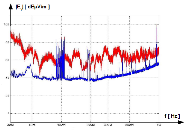
In Fig.1.1 spectrum of the module of the vertical component of the electric field [latex]|E_v|[/latex] in the frequency range from 30 [latex]MHz[/latex] to 1 [latex]GHz[/latex] in one of the the premises at the Technical University of Warsaw is shown. The blue plot represents intentional signals. By 100[latex]MHz[/latex] radio FM broadcasts are visible, by 200 [latex]MHz[/latex] TV channels, above 900[latex]MHz[/latex] signals of the cellular telephony. Moreover services like: emergency medical service, police, fire service are also present. All these signals are useful for functioning of the society but for someone or something incidental they can be disturbing. The red plot is captured by switched on drilling hand tool. Sparks on the commutator of the motor increases significantly level of spectrum in the wide frequency range. It is waste product by operating the tool which is evidently the disturbance and not at all desirable.
It is impossible to remove, compensate or fly away from the electromagnetic environment. Human beings and its artefacts are forced to live and to operate in it without spoiling it excessively, being at the same time immune enough for performance as intended in the presence of it.

Obviously there is interaction between the environment and items embedded in it. Human being can be influenced by the electromagnetic environment through the impact on the health and through undesired theft of electronically processed data.
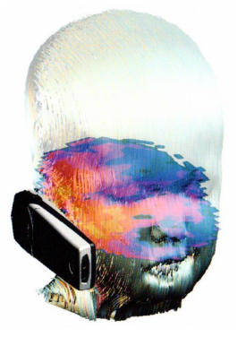
Cellular telephones are example of the impact of the electromagnetic environment on the human being health. In the [latex]90^{th}[/latex] of the [latex]20^{th}[/latex] century, when the first generation of the cellular telephones became the mass consumer good, many customers observed anxious symptoms after long calls. They observed redness and warming up of the head region next to the phone, they filled physical and psycho tiredness. Already then the results of experiments with monkeys were known. They behaved abnormally when temperature of their brains was increased by 1 deg. Very rapidly it was proved that temperature of human brain increases much more extensively by the cellular phone call. Exemplary numerical simulation of energy absorption by cellular phone call is shown in Fig.1.2.
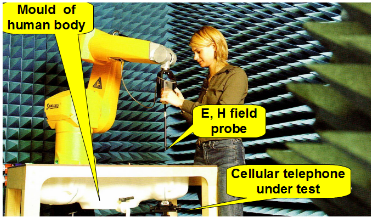
The method for quantification of ability of cellular telephones for warming up the brain tissue was worked out. Specific Absorption Rate SAR which is energy absorbed by the human brain per unit mass was chosen as the quantification parameter. It is measured in [latex]W/m^3[/latex]. In Fig.1.3 the set up for SAR measurement by cellular phone call is shown. It is built in the anechoic chamber laid up with the pyramid absorption material. It consists of mould of the half of human body filled with solution with electric and magnetic properties similar to human brain. Beneath the phone under test is placed. The robot moves the arm with isotropic electric and magnetic near field probes. Measured distribution of both fields in the volume of the brain are recalculated to SAR. All phones available on the marker must contain in the manual the value of its SAR parameter.
The phenomenon described above is direct thermal effect of the phones. Long term influence of the cellular telephones on human being is still under investigation. The answer on this question is unknown.
I wonder if someone realizes that content of the PC monitor emits to the environment. The same happens by scanning or printing something. Processed date are contained in the electromagnetic disturbance leaked out to the surroundings. It is sufficient to place appropriate antenna and receiver and the data can be reconstructed.
Even without antenna the data can be stolen. Emitted data are present in all metal objects in the vicinity. It is enough to mount the current measurement probe on the metal leg of a table placed next to the source of leaked data in order to reconstruct them.
Banks, insurance companies, authorities, secret services, armies spends a lot of money to avoid the thefts of electronically processed data of their customers or citizens. Topics concerning safe data processing are collected under keyword Transient ElectroMagnetic Pulse Emanation Standard TEMPEST.
European regulation relating to electromagnetic compatibility {#EU regulation}
Interaction between electromagnetic environment and items embedded in it is called electromagnetic compatibility EMC.
The laws of the Member States of the European Union relating to electromagnetic compatibility are harmonized according to the so called EMC Directive [@EMCD].
The first sentence in chapter 1 of this Directive sounds: “This Directive regulates electromagnetic compatibility of equipment”. It means that EMC in concept of the Directive is limited to equipment. The human being is left out of the scope of it. The same line is adopted in these lecture notes.
Some other definitions from the first chapter of the Directive [@EMCD] :
- electromagnetic environment means all electromagnetic phenomena observable in the given location,
- electromagnetic compatibility means the ability of equipment to function satisfactorily in its electromagnetic environment without introducing intolerable electromagnetic disturbances to other equipment in that environment,
- electromagnetic disturbance means any electromagnetic phenomenon which may degrade the performance of equipment; an electromagnetic disturbance may be electromagnetic noise, an unwanted signal or a change in the propagation medium itself,
- immunity means the ability of equipment to perform as intended without degradation in the presence of an electromagnetic disturbance.
Though the EMC Directive is limited to equipments, electromagnetic environment according to it covers also natural phenomena in addition to disturbances generated by equipments.
Stipulating that an equipment lives when it is energized, the statement: “live and let live” is good paraphrase of definition of the EMC in the Directive [@EMCD]. It is essential and sole legal requirement of the Directive.
The relationship between standardization and legislation at European level has been developed in accordance with the so-called ‘New Approach’ to technical harmonization and standards. This is cardinal rule regulating the EU market.
According to the New Approach:
- the Countries of the European Union adopts legislation (EU Directives) that defines essential requirements – in relation to safety and other aspects of public interest – which should be satisfied by products and services being sold in the Single Market,
- the European Commission issues standardization requests (Mandates) to the European Standardization Organizations: CEN Comité Européen de Normalisation European Committee for Standardization, CENELEC Comité Européen de Normalisation Electrotechnique European Committee for Electrotechnical Standardization, and ETSI European Telecommunications Standards Institute, which are responsible for preparing technical standards and specifications that facilitate compliance with these essential requirements,
- public authorities of EU countries must recognize that all products manufactured (and services provided) in accordance with harmonized standards are presumed to conform to the essential requirements as defined by the relevant EU legislation,
- European Standards remain voluntary and there is no legal obligation to apply them. Any manufacturer (or service provider) who chooses not to follow a harmonized standard is obliged to prove that his products (or services) conform to the essential requirements.
European Standards remain voluntary but as stated in Chapter 3 of the Directive [@EMCD] “Equipment which is in conformity with harmonised standards shell be presumed to be in conformity with the essential requirements” of the Directive.

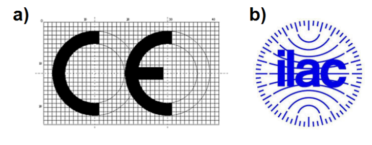
For placing the product on the market the authorized representative of the manufacturer must sign the declaration of conformity. It must be attached to the product. Moreover marking such as in Fig.1.4 a) must be affixed on the product in visible place. CE is abbreviation of the term in French CONFORMITÉ EUROPÉENNE. The authorized representative bears legal responsibility for any violation of the essential requirements concerning the product. The authorized representative means any natural or legal person established within the Union who has written mandate from a manufacturer to act on his behalf.
Implications of the New Approach relating to EMC is establishing plenty of independent accredited laboratories and notified bodies offering services in conformity assessment procedure. EMC testing according to European Standards is the main part of this assessment.
Manufacturer can perform EMC testing with own facility but contracting it to independent accredited laboratory has following benefits:
- liberation from suspicions of lack of objectivity and impartiality,
- test equipment calibrated with traceability,
- educated engineer staff competent to define scope of applicable harmonized standards and to go professionally through the testing program,
- test performance according to valid, not obsolete editions of the harmonized standards,
- accredited test report as the trace that the tested product (DUT Device Under Test, EUT Equipment Under Test ) is in conformity with harmonised standards.
As mentioned before, conformity with harmonised standards is enough to presume that the product is in conformity with the essential requirements of the Directive [@EMCD].
Each Member Country designates accrediting and notifying authority. In Poland it is PCA Polskie Centrum Akredytacji Polish Center for Accreditation. In the home page of the PCA a list of all accredited laboratories with their scope of accreditation can be found. Notified bodies are additionally notified the European Commission and other Member States.
Directive [@EMCD] provides also institution called Market Surveillance Authority of the Member States. In Poland it is Urząd Komunikacji Elektronicznej UKE Office of Electronic Communication.
If the apparatus presents the risk, the Surveillance Authority shell carry out an evaluation. Thereafter shell force the relevant economic operator to take all appropriate corrective actions to bring the apparatus into compliance, to withdraw the apparatus from the market, or to recall it within the reasonable period. If the relevant economic operator does not take adequate corrective actions, the Market Surveillance Authority shell take appropriate provisional measures to prohibit or restrict the being made available, to withdraw it or to recall it. The Surveillance Authority can impose financial penalty.
Accrediting and notifying authorities from many countries around the World, significantly exceeding European Union are associated in the International Laboratory Accreditation Cooperation ILAC. Agreement of ILAC Countries guaranties mutual recognition of the test results performed in the accredited laboratories. For the EU Countries it is tremendous simplification and costs reduction of the conformity assessment procedure. This procedure can be performed only in one EU Country and is recognized elsewhere in EU. The label shown in Fig.1.4 b), placed at the front page of the accredited test report is the seal confirming this.
dB, or not dB, that is the question
Floating decibels
Definitions of floating decibel are as follows
[latex]N \: dB \: (of \, power) \equiv 10\log_{10} \left( \frac {P_2}{P_1} \right) \label{P_dB} \tag{1.1}[/latex]
[latex]N \: dB \: (of \, voltage) \equiv 20\log_{10} \left( \frac {U_2}{U_1} \right) \label{U_dB} \tag{1.2}[/latex]
[latex]N \: dB \: (of \, current) \equiv 20\log_{10} \left( \frac {I_2}{I_1} \right) \label{I_dB} \tag{1.3}[/latex]
[latex]N \: dB \: (of \, electric \, field \, strength) \equiv 20\log_{10} \left( \frac {E_2}{E_1} \right) \label{E_dB} \tag{1.4}[/latex]
[latex]N \: dB \: (of \, magnetic \, field \, strength) \equiv 20\log_{10} \left( \frac {H_2}{H_1} \right) \label{H_dB} \tag{1.5}[/latex]
N is a number. The adjective “floating” means that both values in numerator as well as in denominator can be arbitrary. They are not fixed. Definitions (1.4) and (1.5) concerns vectors. Therefore only one component of electric field respectively magnetic field, e.g. horizontal or vertical component is meant in them.
Inverse calculation is as follows
[latex]\frac{P_2}{P_1} = 10^{\frac{N \: dB}{10}} \label{P2_P1} \tag{1.6}[/latex]
[latex]\frac{U_2}{U_1} = 10^{\frac{N \: dB}{20}} \label{U2_U1} \tag{1.7}[/latex]
[latex]\frac{I_2}{I_1} = 10^{\frac{N \: dB}{20}} \label{I2_I1} \tag{1.8}[/latex]
[latex]\frac{E_2}{E_1} = 10^{\frac{N \: dB}{20}} \label{E2_E1} \tag{1.9}[/latex]
[latex]\frac{H_2}{H_1} = 10^{\frac{N \: dB}{20}} \label{H2_H1} \tag{1.10}[/latex]

It is clear that 10-tuple change of power means change about [latex]10dB[/latex], Eq.1.1. It must be also clear that 10-tuple change of voltage, current or field strength means change about [latex]20dB[/latex], Eqs.: 1.2, 1.3, 1.4, 1.5 .
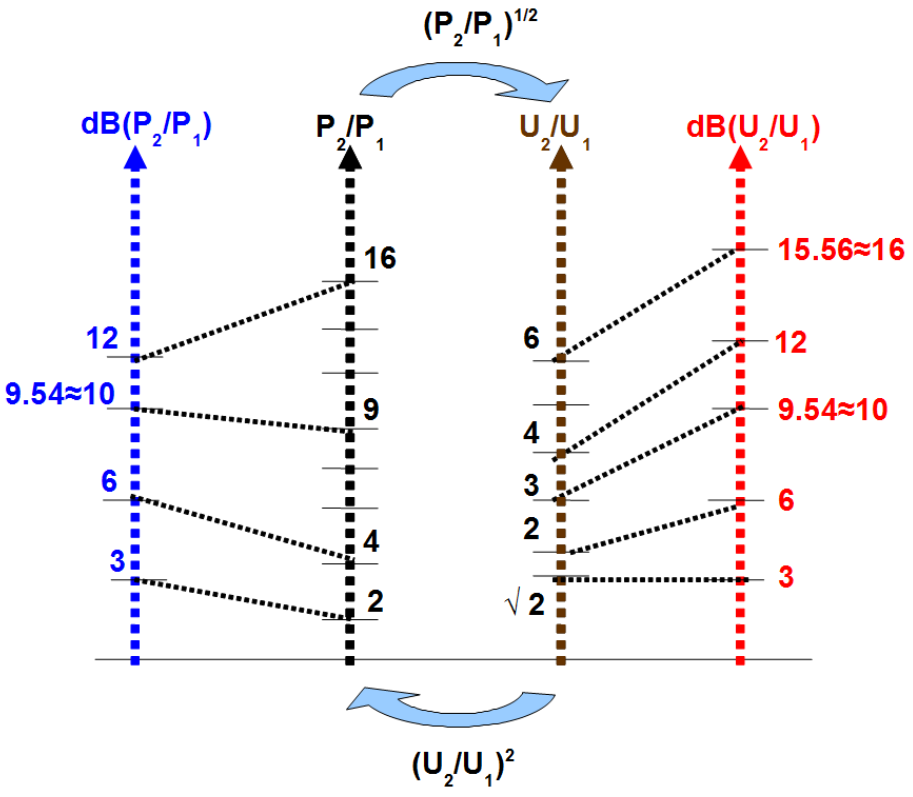
Moreover it is advisory to remember some other selected relations between linear and dB scale. They are shown in Fig.1.5. Ratio 2 and 3 in linear scale of voltage (brown axis) corresponds respectively with [latex]6dB[/latex] and [latex]9.54dB[/latex], Eq.1.2 which is almost equal to [latex]10dB[/latex](red axis). The same concerns definitions (Eq.: 1.3), (1.4), (1.5).
Exception is power due to multiplier 10 before [latex]\log[/latex] Def.(Eq.1.1). Ratio 2 and 9 in linear scale of power (black axis) corresponds respectively with [latex]3dB[/latex] and [latex]9.54dB[/latex], Eq.1.1 which is almost [latex]10dB[/latex](blue axis).
Usually explanation in parentheses behind [latex]dB[/latex] symbol is omitted. It is redundant due to clever use of multiplier 10 by power and 20 by remaining definitions of [latex]dB[/latex].

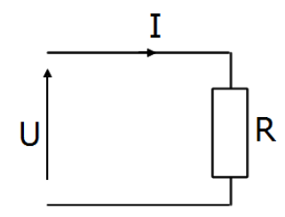
For any one-port as shown in Fig.1.6 relation between power, voltage and current is as follows
[latex]P_1 = \frac {U_1^2}{R} = R I_1^2[/latex]
[latex]P_2 = \frac {U_2^2}{R} = R I_2^2 \label{Power_U_I} \tag{1.12}[/latex]
where [latex]R[/latex] is resistance of the one-port.
Any change of power by the ratio [latex]P_2/P_1[/latex] is coupled with following changes of voltage and current
[latex]N \: dB = 10\log_{10} \left( \frac {P_2}{P_1} \right) = 10\log_{10} \left( \frac {U_2}{U_1} \right)^2 = 20\log_{10} \left( \frac {U_2}{U_1} \right)[/latex]
[latex]N \: dB = 10\log_{10} \left( \frac {P_2}{P_1} \right) = 10\log_{10} \left( \frac {I_2}{I_1} \right)^2 = 20\log_{10} \left( \frac {I_2}{I_1} \right) \label{N_dB} \tag{1.14}[/latex]
Conclusions from Eqs.(1.14) can be generalized. Any change of power about N [latex]dB[/latex] causes change of voltage, current or field strength also about N [latex]dB[/latex].
It can be interpreted in Fig.1.5. Let’s say that voltage is increased about [latex]3dB[/latex] (red axis). It means that it is increased by ratio [latex]\sqrt{2}[/latex] Eq.1.7, (brown axis). By jumping from voltage axis (brown axis) to power axis (black axis) operator “power 2” must be applied, due to Eq.1.12. [latex]\sqrt{2}[/latex] in brown axis is coupled with [latex]2[/latex] on black axis. Finally it is coupled with [latex]3dB[/latex] on blue axis, Eq.1.1.
An example in opposite direction. Let’s say that power is increased about [latex]12dB[/latex] (blue axis). It means that it is increased by ratio [latex]16[/latex] (black axis), Eq.1.6. By jumping from power axis (blue axis) to voltage axis (blown axis) operator “square root of 2” must be applied, due to Eq.1.12. [latex]16[/latex] in black axis is coupled with [latex]4[/latex] on brown axis. Finally it is coupled with [latex]12dB[/latex] Eq.1.1 on red axis.
Bound decibels
Despite floating decibels very often decibels with fixed value in denominator are used. Most commonly decibels are bound to
[latex]N \: dB[mW] \equiv 10\log_{10} \left( \frac {P}{1mW} \right) \label{mW_dB} \tag{1.15}[/latex]
[latex]N \: dB[\mu V] \equiv 20\log_{10} \left( \frac {U}{1\mu V} \right) \label{uV_dB} \tag{1.16}[/latex]
[latex]N \: dB[\mu A] \equiv 20\log_{10} \left( \frac {I}{1\mu A} \right) \label{uA_dB} \tag{1.17}[/latex]
[latex]N \: dB[\mu V/m] \equiv 20\log_{10} \left( \frac {E}{1 \frac {\mu V}{m}} \right) \label{uVm_dB} \tag{1.18}[/latex]
[latex]N \: dB[\mu A/m] \equiv 20\log_{10} \left( \frac {H}{1 \frac{\mu A}{m}} \right) \label{uAm_dB} \tag{1.19}[/latex]
Equivalently [latex]dB[m][/latex] is often used in definition (1.15). Moreover the square brackets can be omitted. Do not be astonished meeting notations like [latex]dBm[/latex], [latex]dB\mu V[/latex], [latex]dB\mu V/m[/latex].
The denominator is the reference value. Number N says about how many [latex]dB[/latex] is the value in question (in numerator) bigger or smaller than the reference value in denominator.
In another way one can say, that decibel is bound the reference value in denominator.
Inverse calculation is as follows
[latex]P \:[mW] = 10^{\frac{N \: dBmW}{10}} \label{P_mW} \tag{1.20}[/latex]
[latex]U \: [\mu V] = 10^{\frac{N \: \mu V}{20}} \label{U_uV} \tag{1.21}[/latex]
[latex]I \: [\mu A] = 10^{\frac{N \: \mu A}{20}} \label{I_uV} \tag{1.22}[/latex]
[latex]E \: [\mu V/m] = 10^{\frac{N \: \mu V/m}{20}} \label{E_uVm} \tag{1.23}[/latex]
[latex]H \: [\mu A/m] = 10^{\frac{N \: \mu A/m}{20}} \label{H_uAm} \tag{1.24}[/latex]
There is still another group of bound decibels such as [latex]dB_i[/latex], [latex]dB_{\lambda/2}[/latex], [latex]dB_d[/latex] and [latex]dB_c[/latex]. In the first one the reference is the isotropic antenna. The second and the third are equivalent and concerns the dipole antenna. [latex]dB_c[/latex] concerns content of the harmonics in the RF signal for which the main harmonic i.e. carrier signal is the reference. This group of bound decibels will be presented in the later part of the course.
Good exercise for surfing in the decibel world is calculation of relation between power in [latex]dBm[/latex] and voltage in [latex]dB\mu V[/latex] for the one-port as shown in Fig.1.6.
Voltage – power relation yields [latex]U^2 = R \cdot P \label{107dB_1}\tag{1.25}[/latex]
Nothing will change if the left hand side will be divided by [latex](1\mu V)^2[/latex] and multiplied by [latex](1\mu V)^2[/latex] i.e. by [latex]10^{-12}V^2[/latex] and the right hand side will be divided by [latex]1mW[/latex] and multiplied by [latex]1mW[/latex] i.e. by [latex]10^{-3}W[/latex]
[latex]U^2 \cdot \frac{10^{-12} V^2}{(1\mu V)^2} = R \cdot P \cdot \frac{10^{-3} W}{1mW} \label{107dB_2}\tag{1.26}[/latex]
Rearranging yields [latex]\left( \frac{U}{1\mu V} \right)^2 = \frac{R}{1\Omega} \cdot \frac{P}{1mW} \cdot 10^{9} \label{107dB_3}\tag{1.27}[/latex]
Logarithmising both side of equality with 10-tuple logarithm to base 10 yields
[latex]20 \log \left( \frac{U}{1\mu V} \right) = 10 \log \left( \frac{R}{1\Omega} \right) + 90 + 10 \log \left( \frac{P}{1mW} \right) \label{107dB_4}\tag{1.28}[/latex]
Finally for resistance [latex]R=50 \Omega[/latex] [latex]U_{dB\mu V} \approx 107 + P_{dBmW} \label{107dB}\tag{1.29}[/latex]
Electrical dimension
Physical dimensions of a radiating structure such as antenna are not important in determining the ability of that structure to transmit or receive electromagnetic energy. Electrical dimension, meant as ratio of physical dimensions of the structure to the wavelength [latex]\lambda[/latex] feeding it or induced in it are more significant in determining this ability.
Similarly, by transporting energy or transmitting signal with a line, physical length of the line does not rule presence of wave propagation along it. Again electrical length, meant as physical length of the line related to the wavelength [latex]\lambda[/latex] of the transported energy or transmitted signal is relevant in respect of it.
In [@Clayton] the criterion for electrically small circuit is defined. Circuit is electrically small if its largest dimension is smaller then one-tenth of a wavelength accompanied with signal or energy processed with the circuit. In such case distributed nature of the electromagnetic field can be ignored and lumped circuit models are an adequate representation of the electromagnetic phenomena. This criterion includes also electrically short line which can be represented with the lumped circuit, unlike electrically long line which must be represented with distributed parameters.
This criterion is applied in everyday engineer life. Nowadays oscilloscopes have optional setting of the input resistance [latex]50\Omega[/latex] or [latex]1M\Omega[/latex]. If the cable in the measurement path is electrically short then it doesn’t matter which setting is chosen. However if the cable in the measurement path is electrically long it must be viewed as distributed line in which the wave is propagating. In such a case distortion-free measurement of the signal is assured only by setting [latex]50\Omega[/latex] input resistance. Usually cable in the measurement path is coaxial one with [latex]50\Omega[/latex] characteristic impedance. Its [latex]50\Omega[/latex] termination at the oscilloscope input enables to avoid mismatching.
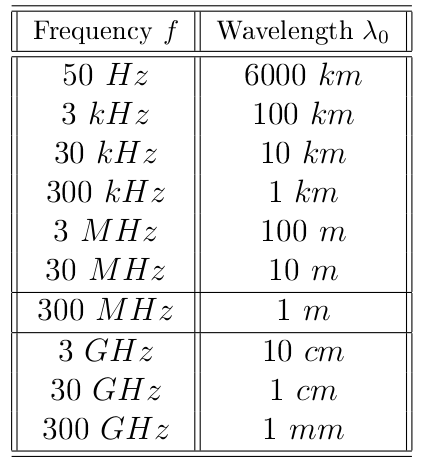
In Table 1.1 wavelength in vacuum for different frequencies are gathered. It is beneficial to learn by hard one row of that table [latex]f=300MHz \: \Rightarrow \: \lambda_0=1m[/latex]. It is good reference for estimating the wavelength by other frequencies.
[[Dlugosc fali]]{#Dlugosc fali label=“Dlugosc fali”}
The velocity of propagation in free space in vacuum is
[latex]v_0 = \frac{1}{\sqrt{\varepsilon_0\mu_0}} \approx 3 \cdot 10^8 m/s \label{v_0}\tag{1.30}[/latex]
where [latex]\varepsilon_0 \approx 8.854 \cdot 10^{-12}[/latex] [latex]F/m[/latex], [latex]\mu_0 \approx 4\pi \cdot 10^{-7}[/latex] [latex]H/m[/latex].
In other media with relative parameters [latex]\mu_r[/latex], [latex]\varepsilon_r[/latex] not equal to 1, it is
[latex]v = \frac{1}{\sqrt{\varepsilon\mu}} = \frac{v_0}{\sqrt{\varepsilon_r\mu_r}} \label{v_propagation}\tag{1.31}[/latex]
For example, a wave propagation in Teflon ([latex]\varepsilon_r=2.1[/latex], [latex]\mu_r=1[/latex]) has a velocity of propagation of [latex]v=0.69 \cdot v_0[/latex]. Accordingly, the wavelength in Teflon is shortened by factor [latex]0.69[/latex].
If the frequency band of the signal measured with the oscilloscope goes up to [latex]100MHz[/latex] and cable in the measurement path is [latex]50\Omega[/latex] Teflon cable, then the wavelength in the cable is [latex]2.07m[/latex]. Available coaxial cables have length of [latex]0.5m[/latex], [latex]1.0m[/latex] or more. It is obvious that in such case they are electrically long and oscilloscope setting must be practically always [latex]50\Omega[/latex].
In standard [@EN-4-20] another definition of electrical dimension is introduced. The context of it is the size estimation of the device which can be measured in the Gigahertz Transverse Electromagnetic GTEM cell. Device is electrically small if its largest dimension is smaller than one wavelength at the highest frequency for which the measurement should be done.
Both definitions introduced in [@Clayton] and in [@EN-4-20] are only rules of thumb and as such can better or worse estimate reality depending on situation.
Power (impedance) matching {#impedance maching}
 Considered is the circuit in Fig. 1.7 a). Let us assume the internal source resistance as parameter [latex]R_S = const[/latex] and variable load resistance [latex]R_L=var[/latex].
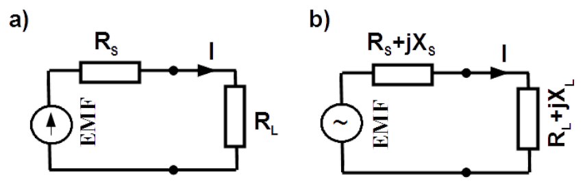
Power delivered from the source to the circuit in Fig. 1.7 a) is [latex]P(R_L) = EMF \cdot I = \frac{EMF^2}{R_S + R_L}[/latex]
Power dissipated in the load is
[latex]P_{L}(R_L) = R_L \cdot I^2 = \frac{R_L \cdot EMF^2}{(R_S + R_L)^2} \label{P_L}\tag{1.33}[/latex]
Power losses in the source are
[latex]P_{S}(R_L) = R_S \cdot I^2 = \frac{R_S \cdot EMF^2}{(R_S + R_L)^2}[/latex]
The source has unlimited capability but it delivers power as demanded by the load. In order to figure out how big is maximal demanded power, extremum condition on variable [latex]P_L(R_L)[/latex] in Eq. (1.33) must be imposed. The answer is [latex]R_S = R_L[/latex]. This is called power or impedance matching condition.
By matching, the load absorbs maximal power from the source [latex]P_{L_{max}} = \frac{EMF^2}{2 R_S} \label{P_max}\tag{1.35}[/latex]
The same amount of power is dissipated in the internal source resistance [latex]R_S[/latex].
Budget of power can be explained with incident and reflected power. The source sends incident power [latex]P_{L_{max}}[/latex] to the load. If the load is ready to absorb the whole amount of delivered power i.e. matching condition is fulfilled, then it does it. Otherwise part of the incident power is reflected from the load and travels back to the source. The net power dissipated in the load is equal to the incident power decreased about the reflected power. The same happens to the power delivered from the source.
Let us introduce variable [latex]k[/latex] as quotient of the load and the source resistance [latex]k = R_L / R_S[/latex]. Moreover let us define variable: power dissipated in the load related to the maximal power that can be absorbed in the load, see Eq. (1.35)
[latex]p_L(k) = \frac{P_L (k)}{P_{L_{max}}} = \frac{4k}{(1 + k)^2}[/latex]
along with variable: power losses in the source related to the maximal power that can be absorbed in the load, see Eq. (1.35)
[latex]p_S(k) = \frac{P_S (k)}{P_{L_{max}}} = \frac{4}{(1 + k)^2}[/latex]
Finally let us define efficiency as the ratio of power dissipated in the load and delivered from the source
[latex]\eta(k) = \frac{P_L (k)}{P} = \frac{k}{(1 + k)}[/latex]

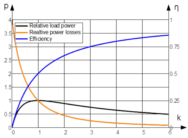
[latex]p_L(k)[/latex], [latex]p_S(k)[/latex] and [latex]\eta(k)[/latex] are presented in Fig.1.8. In the distinctive point, by matching ([latex]k=1[/latex]) both relative powers are equal 1. The efficiency in that point is equal 0.5.
Power electro engineers are accustomed with coefficient [latex]k \gg 1[/latex]. They cannot design generators which deliver maximal power to the load with 50 [latex]\%[/latex] of internal losses. They try to operate in the region by which efficiency [latex]\eta[/latex] is approaching 1. Indeed, delivered power is smaller there than maximal [latex]P_{L_{max}}[/latex] but in the same time losses are suppressed, so that efficiency is big.
On the contrary, electronic engineers pursuit of matching point ([latex]k=1[/latex]). Never mind that they have to provide twice as much power as they require. Matching for them is indispensable. They operate in the frequency range in which lines for transmitting signal or power must be regarded as distributed lines. Due to frequency dependence of the input impedance of a transmission lines, the line which is open circuited at the end can have input impedance close to zero. RF signal generators and amplifiers are not design to sustain the short circuit.
Matching condition for the AC circuit shown in Fig. 1.7 b) can be explained in two steps:
- imaginary part of impedance [latex]\bf{Z_S}[/latex] must be equal to the conjugate of the imaginary part of [latex]\bf{Z_L}[/latex] ([latex]jX_S = -jX_L[/latex])1.
- real parts of [latex]\bf{Z_S}[/latex] and [latex]\bf{Z_L}[/latex] (resistances [latex]R_S[/latex] and [latex]R_L[/latex]) must be equal one to another. This results from the same consideration as for the DC circuit.

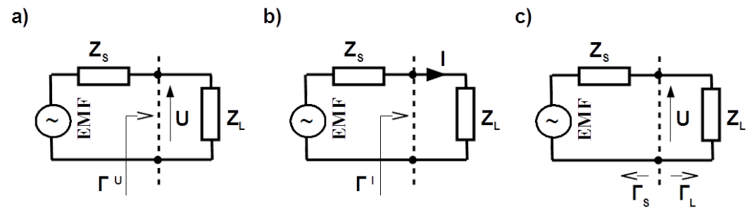
Voltage [latex]{\bf{U}}[/latex] across the load in Fig. 1.9 a) can be expressed with the Omh’s and the Kirchhoff’s circuit laws
[latex]{\bf {U}} = \frac{{\bf{Z_L }}}{{\bf{Z_S}} + {\bf{Z_L}}} {\bf {EMF}}= {\bf {U_i}} + {\bf {U_r}} \label{GAMMA_1}\tag{1.39}[/latex]
Similar as for power this voltage can be split into incident and reflected component: [latex]{\bf {U_i}}[/latex] and [latex]{\bf {U_r}}[/latex] respectively. The first is meant as voltage that would be receipted by the load in case of matching to the source impedance ([latex]{\bf{Z_L}} = {\bf{Z_S}}^*[/latex]). It will be [latex]{\bf{U_i}} = {\bf {EMF}}/2[/latex]. In order to fulfill Eq.(1.39) reflected voltage yields [latex]{\bf {U_r}} = \frac{{\bf{Z_L}} - {\bf{Z_S}}}{{\bf{Z_L}} + {\bf{Z_S}}}\cdot \frac{{\bf {EMF}}}{2}[/latex]
[latex]{\bf {U_r}}[/latex] is the voltage reflected by the load in case of mismatching and sent back to the source.
Voltage reflection coefficient is defined as quotient of reflected and incident voltage ([latex]{\bf {\Gamma}}^U = {\bf {U_r}}/{\bf {U_i}}[/latex]).
[latex]{\bf {\Gamma}^U} = \frac{{\bf{Z_L }} - {\bf{Z_S }}}{{\bf{Z_L}} + {\bf{Z_S}}} \hspace{1.5cm} {\bf{Z_L}} = \frac{1 + {\bf {\Gamma}^U}}{1 - {\bf {\Gamma}^U}} \label{GAMMA_2}\tag{1.41}[/latex] With rearrangement the load impedance can be derived.
Analogue the current reflection coefficient can be derived for the circuit in Fig. 1.9 b). [latex]{\bf {I}} = \frac{\bf {EMF}}{{\bf{Z_L}} + {\bf{Z_S}}} = {\bf {I_i}} + {\bf {I_r}} \label{GAMMA_3}\tag{1.42}[/latex]
The incident current will be [latex]{\bf{I_i}} = {\bf {EMF}}/2 {\bf{Z_S}}[/latex]. In order to fulfill Eq.(1.42) reflected current yields [latex]{\bf {I_r}} = - \frac{{\bf{Z_L}} - {\bf{Z_S}}}{{\bf{Z_L}} + {\bf{Z_S}}}\cdot \frac{{\bf {EMF}}}{2 {\bf{Z_S}}}[/latex]
Current reflection coefficient is defined as quotient of reflected and incident current ([latex]{\bf {\Gamma}}^I = {\bf {I_r}}/{\bf {I_i}}[/latex]).
[latex]{\bf {\Gamma}^I} = - \frac{{\bf{Z_L }} - {\bf{Z_S }}}{{\bf{Z_L}} + {\bf{Z_S}}} \hspace{1.5cm} {\bf {\Gamma}^I} = - {\bf {\Gamma}^U} \label{GAMMA_4}\tag{1.44}[/latex]
[latex]{\bf {\Gamma}^I}[/latex] is rarely used. Lack of upper case in symbol means the voltage coefficient.
Reflection coefficient is always related to some impedance. Up to now reference was the source impedance [latex]{\bf {Z_S}}[/latex]. Generally it can be arbitrary impedance [latex]{\bf {Z_0}}[/latex] causing reflection in both directions: toward the source [latex]{\bf{\Gamma_S}} =({\bf {Z_S}} - {\bf {Z_0}})/({\bf {Z_S}}+{\bf {Z_0}})[/latex] and toward the load [latex]{\bf{\Gamma_L}} = ({\bf {Z_L}} - {\bf {Z_0}})/({\bf {Z_L}}+{\bf {Z}}_0)[/latex] as shown in Fig. 1.9 c). Majority of measurement instruments are referred to resistance [latex]{\bf {Z_0}} = 50[/latex] [latex]\Omega[/latex].
Very easily following relation between reflection coefficients can be derived
[latex]\frac{{\bf {Z}}_S }{{\bf {Z}}_L } = \frac{1 + {\bf {\Gamma}}_S}{1 + {\bf {\Gamma}}_L }\cdot \frac{1 - {\bf {\Gamma}}_L} {1 - {\bf {\Gamma}}_S}[/latex]
Finally [latex]{\bf {U}} = \frac{{\bf{EMF}}}{1 + \frac{{\bf {Z_S}}}{{\bf {Z_L}}}} = \frac{(1-{\bf {\Gamma}}_S )( 1+{\bf {\Gamma}}_L )}{1- {\bf {\Gamma}}_S {\bf {\Gamma}}_L} \cdot \frac{{\bf {EMF}}}{2} \label{U}\tag{1.46}[/latex]
This voltage looks much more friendly in dependence on impedances, see Eq.(1.39). Derivation of it in dependence on reflection coefficients seems to be scholastic exercise but it is not the case. Mind that in RF technique direct measurement of impedances and resistances unlike reflection coefficients is not possible.
Attenuation (transmission) vs. voltage division factor
Insertion loss [latex]{\bf{L}}_i[/latex] of a two-port illustrated in Fig. 1.10 as Device Under Test (DUT) is ratio of voltages across the load impedance [latex]{\bf{Z}}_L[/latex], which terminates the DUT in two situations, when:
- the load [latex]{\bf{Z}}_L[/latex] is connected directly to the source, [latex]{\bf{U}}[/latex] in Fig. 1.10 a),
- between the load and the source the DUT is inserted, [latex]{\bf{U}}_2[/latex] in Fig. 1.10 b).
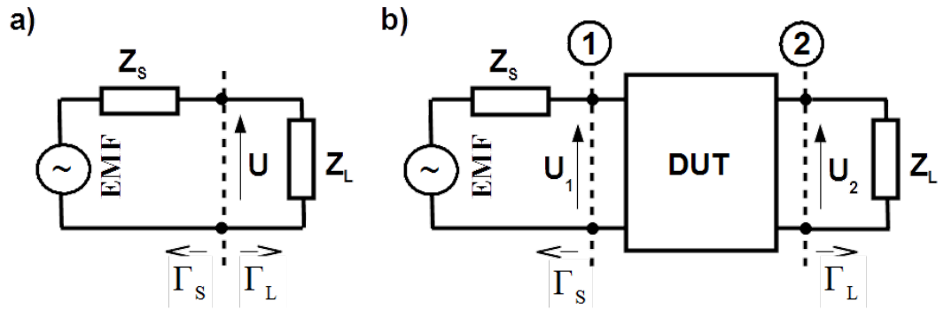
Insertion loss [latex]{\bf {L}}_i = {\bf{U}}/{\bf{U}}_2[/latex] depends on the source [latex]{\bf{Z}}_S[/latex] and the load [latex]{\bf{Z}}_L[/latex] impedance.
Attenuation of a DUT is insertion loss under matching regime at the source and the load ([latex]{\bf{Z}}_S = {\bf{Z}}_L = {\bf{Z}}_0[/latex])2. Transmission is inverse of the attenuation.
For reciprocal DUTs e.g. passive, linear DUTs attenuation [latex]{\bf{A}}_{12}[/latex] from port 2 to 1 (source applied to port 1, see Fig. 1.10 b)) and in opposite direction [latex]{\bf{A}}_{21}[/latex] ( source applied to port 2) are the same
[latex]{\bf{A}}_{12} = {\bf{A}}_{21} \label{L_i2}\tag{1.47}[/latex] Memorise that attenuation is referred to the source and load impedance equal to [latex]{\bf{Z}}_0[/latex].
Voltage loss [latex]{\bf{L}}_v[/latex] of a two-port illustrated in Fig. 1.10 b) as Device Under Test (DUT) is ratio of input voltage [latex]{\bf{U}}_1[/latex] and output voltage [latex]{\bf{U}}_2[/latex].
Voltage loss [latex]{\bf {L}}_v = {\bf{U}}_1/{\bf{U}}_2[/latex] depends only on the load [latex]{\bf{Z}}_L[/latex] impedance.
Voltage division factor of a DUT is voltage loss under matching regime at the load ([latex]{\bf{Z}}_L = {\bf{Z}}_0[/latex])
[latex]{\bf{VDF}} = {\bf{L}}_{v_{|_{{\bf{\Gamma}_L}=0}}} \label{L_v}\tag{1.48}[/latex]

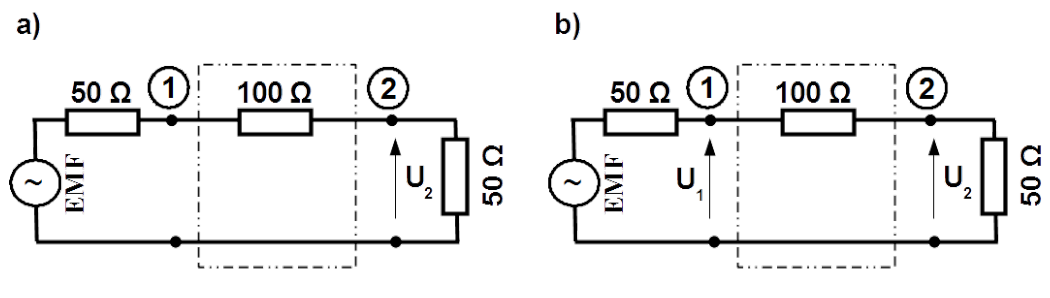
Let us calculate attenuation of the two-port shown in Fig. 1.11 a), referred to [latex]50[/latex] [latex]\Omega[/latex] resistance. Since [latex]{\bf {U}} = {\bf{EMF}}/2[/latex] and [latex]{\bf {U}}_2 = {\bf{EMF}}/4[/latex] hence [latex]{\bf{A}}_{12} = 2[/latex] i.e. ([latex]6 dB[/latex]).
In Fig. 1.11 b) [latex]{\bf{U}}_2 = {\bf{U}}_1 /3[/latex] then [latex]{\bf{VDF}} = 3[/latex] i.e. ([latex]10 dB[/latex]).
Memorise that attenuation and voltage division factor are different quantities. Apply them consciously, do not confound them!
Let us exercise once more calculation of attenuation referred to [latex]50[/latex] [latex]\Omega[/latex] resistance, illustrating simultaneously the reciprocity principle. The considered two-port has topology with [latex]100[/latex] [latex]\Omega[/latex] serial resistance and [latex]1[/latex] [latex]\Omega[/latex] resistance parallel to the port 2, as shown in Fig. 1.12.
In both cases voltage across the load without insertion of the two-port [latex]U = EMF/2[/latex].

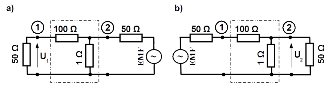
[latex]U_1[/latex] by calculation of [latex]A_{12}[/latex] in the circuit in Fig. 1.12 a) is as follows
[latex]U_1 = \frac{EMF}{50 \Omega + \frac{150 \Omega^2}{151 \Omega}} \cdot \frac{150 \Omega^2}{151 \Omega} \cdot \frac{50 \Omega}{150 \Omega} = \frac{EMF}{154}[/latex] Finally [latex]A_{12} = U/U_1 = 77[/latex].
[latex]U_2[/latex] by calculation of [latex]A_{21}[/latex] in the circuit in Fig. 1.12 b) is as follows
[latex]U_2 = \frac{EMF}{150 \Omega + \frac{50 \Omega^2}{51 \Omega}} \cdot \frac{50 \Omega^2}{51 \Omega} = \frac{EMF}{154}[/latex] [latex]A_{21} = U/U_2 = 77 = A_{12}[/latex], quod erat demonstrandum (q.e.d.)!
What actually R,L,C one-ports are?
In this section examples of frequency characteristics of the passive assembly component RLC are gathered. The aim of it is to evoke strong and everlasting impression that depending on the frequency, even such simple components exhibits any electric properties but that for what they are designed.
Wire wound resistor
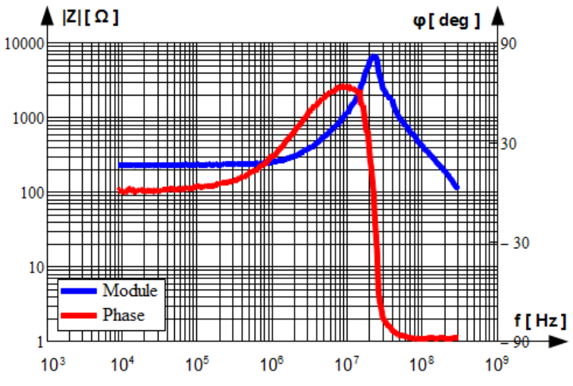
In Fig.1.13 impedance of resistor with rated resistance 216 [latex]\Omega[/latex] made of resistive wire in Through Hole Technology [latex]THD[/latex] is shown. It is measured in the frequency range from 9 kHz to 300 MHz. Actually it is resistance only up to 100 kHz. Its module is equal to rated value and phase is almost equal to zero. From that frequency on inductive character appears. Module and phase rises. Between 20 MHz and 30 MHz there is parallel resonance. Above that frequency module decreases, phase as well reaching [latex]-90^\circ[/latex] i.e. resistor becomes capacitor.
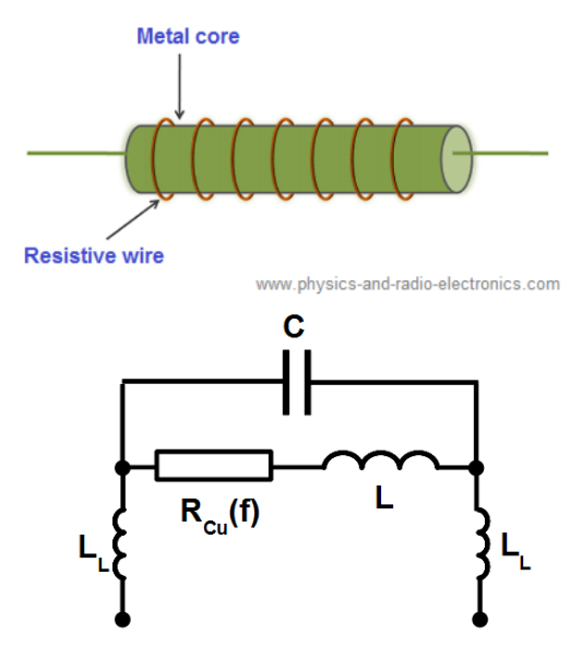
Such plots are clear by focusing on building technology of the resistor. It is shown in Fig.1.14. Wire with circular cross-section wound on the cylindrical former exhibits inductance in addition to resistance. Therefore serial branch [latex]R_{Cu}(f)L[/latex]. Resistance is frequency dependent due to skin effect . There exist also capacitance between turns of wire. Actually there is matrix of all two turns combinations. One capacitance [latex]C[/latex] shown in Fig.Fig.1.14 is simplified model. Two inductances [latex]L_L[/latex] represents inductances of the resistor leads. They are negligible small in comparison to the inductance [latex]L[/latex] of the wound wire.

Metal film resistor
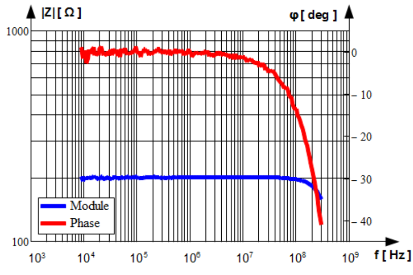
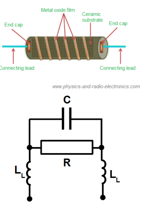
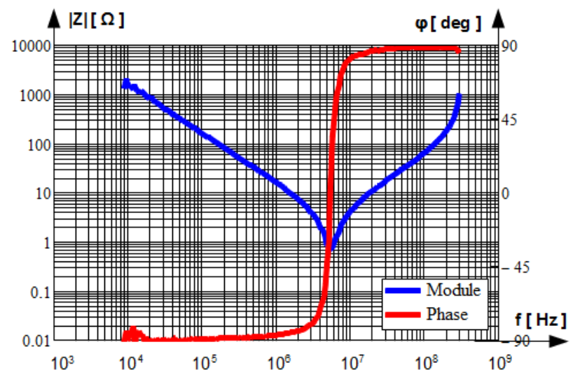
In Fig.1.15 impedance of the THD metal film resistor with rated resistance 200 [latex]\Omega[/latex] is shown. Impedance of this resistor does not exhibit inductive but capacitive character by increasing frequency. This suggests serial resonance by frequency significantly far above [latex]300MHz[/latex]. Explanation lays also in building technology.
Resistance is build with metal oxide sheet etched on the ceramic substrate. Etching due to geometry i.e. rectangular cross-section with width much bigger than height is low inductive, practically non inductive. The metal sheet is encapsulated on both ends in metal caps which serves as the junction between the sheet and the leads. Caps due to relatively big layer oriented parallel one to another build flat condenser which is represented with capacitance [latex]C[/latex] parallel to resistance [latex]R[/latex] in the equivalent circuit in Fig.1.16. Resonance frequency of the serial branch [latex]2L_L C[/latex] which is [latex]f_0=1/\sqrt{2L_L C}[/latex] is much above [latex]300MHz[/latex] due to small values of leads inductances [latex]L_L[/latex]. Influence of the skin effect on the resistance of the metal sheet can be neglected due to rectangular cross-section with width much bigger than height.


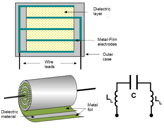
Film capacitor
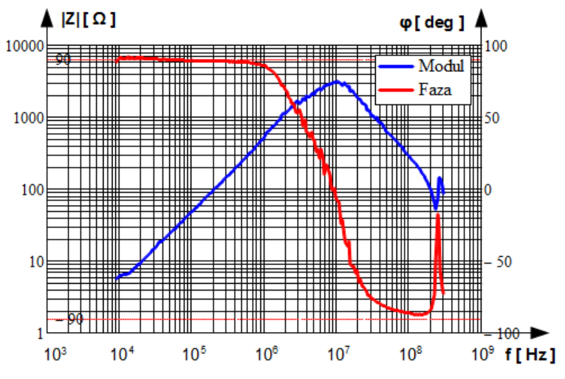
In Fig.1.17 impedance of a THD metal film condenser with rated capacitance 10 [latex]nF[/latex] is shown. Again plot suggests serial resonance between capacitance [latex]C[/latex] for what this one-pole is built and the leads inductances [latex]L_L[/latex]. The resonance frequency falls upon much smaller frequency than in the case of the film resistor, in this case between 5 [latex]MHz[/latex] and 6 [latex]MHz[/latex], because capacitance is significantly bigger.


High frequency choke
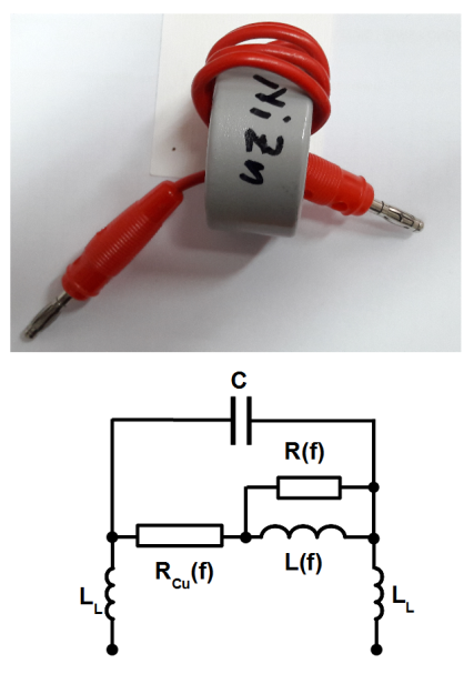
In Fig.1.19 impedance of a high frequency choke built with 4 [latex]mm[/latex] diameter laboratory cable wound on the MnZn toroidal core is shown. The core material exhibits frequency dependent inductance [latex]L(f)[/latex] and frequency dependent losses [latex]R(f)[/latex]. In the low frequency range material is lossless and inductance is constant. Impedance rises with the slope 20 [latex]dB/dec[/latex]. However by frequency about 2 [latex]MHz[/latex] fall of inductance accompanied with rise of losses reveals. Capacitance between turns causes parallel resonance with the choke inductance [latex]L(f)[/latex] by 10 [latex]MHz[/latex]. Resistances representing losses in the core material [latex]R(f)[/latex] and conducting losses in the turns [latex]R_{Cu}(f)[/latex] suppresses resulting resistance by the resonance. Above the parallel resonance the circuit has capacitive character. Another serial resonance between capacitance [latex]C[/latex] and leads inductances [latex]L_L[/latex] is observed above 200 [latex]MHz[/latex].


In bush of the pulse parameters
Pulses are usually captured in the time domain with the single shot oscilloscopes. Nowadays the oscilloscopes have ability to activate cursors for direct measuring of arbitrary instantaneous value of the pulse and the instant. This enables to cope with the pulse parameters. Unfortunately there is really bush by their definitions. The terms are used very often without reflection what they really are? Devoting some time for that section helps to avoid misunderstanding in discussions and to prevent from drawing ill conclusions.
Measurable pulse parameters
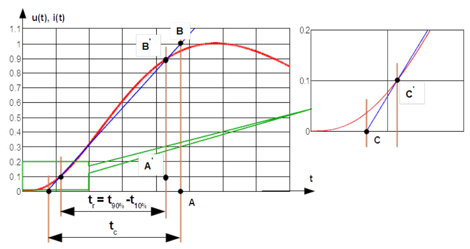
The primary measurable pulse parameter is the pulse peak defined as the first maximum of the wave shape. Remaining parameters i.e. the pulse rise time and the pulse width can be derived from it.
The pulse rise time is the time elapsed between two instants for which instantaneous values of the pulse gets predefined part of the pulse peak. In most cased [latex]90\%[/latex] and [latex]10\%[/latex] of the peak value are used. It is called then [latex]t_r= t_{90\%-10\%}[/latex] as shown in Fig.1.21. In some cases [latex]t_{90\%-30\%}[/latex] is applied. Less frequently [latex]t_{80\%-20\%}[/latex] is used.
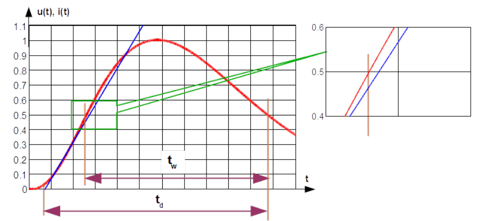
The pulse width is the time elapsed between instants for which instantaneous values of the pulse gets predefined part of the pulse peak on rising slope and on falling slope of the pulse tail. In common use is [latex]t_w= t_{50\%}[/latex] as shown in Fig.1.22.

Calculable pulse parameters
From the measurable parameters other parameters can be calculated.
For calculating the pulse crest (front) time [latex]t_c[/latex] 3 the secant passing through the points constituting the rise time must be built. See blue line in Fig.1.21 which crosses the pulse by [latex]90\%[/latex] and [latex]10\%[/latex] of its peak value. The pulse crest (front) time is the time elapsed between two instants for which the secant reaches the peak value and crosses the time axis.
Relation between lengths of sides of similar triangles [latex]AB/CA =A^{'}B^{'}/C^{'}A^{'}[/latex], particularly [latex]1/t_c =(0.9-0.1)/t_r[/latex] in case shown in Fig.1.21 yields
[latex]t_c= \left\{ \begin{array} {ll} 1.25 \cdot t_r & \mbox{ for t_r = t_{90%-10%} }\\ 1.67 \cdot t_r & \mbox{ for t_r = t_{90%-30%} or t_r = t_{80%-20%}} \end{array} \right. \label{t_c}\tag{1.51}[/latex]
The same secant is used for calculation of the pulse duration [latex]t_d[/latex]. The pulse duration is the time elapsed between instants on the tail when the pulse decreases to [latex]50\%[/latex] of the the peak value and the instant when secant crosses the time axis. See Fig.1.22. Sometime the pulse duration is used interchangeably with the pulse width, causing ambiguity.
Fourier transformations
Fourier series is a way to decompose any periodic function [latex]c(t)[/latex] into the weighted sum of a (possibly infinite) set of simple oscillating functions, namely sines and cosines
[latex]c(t) = a_0 + \sum_{n=1}^{\infty} \left[ A_n \cos( n\omega_1 t) + B_n \sin( n\omega_1 t) \right] \label{cab}\tag{1.52}[/latex]
The first term in series, [latex]n=1[/latex] is called fundamental harmonic and [latex]\omega_1[/latex] angular fundamental frequency. It is related with fundamental frequency [latex]f_1[/latex] and fundamental period [latex]T_1[/latex] as follows
[latex]\omega_1 = \frac{2\pi}{T_1} = 2\pi f_1 \label{omega_1}\tag{1.53}[/latex]
Frequency of n-th harmonic is n-tuple of fundamental frequency.
Coefficients of the Fourier series are as follows
[latex]a_0 = \frac{1}{T_1} \int_{0}^{T_1} c(t) dt \label{a0}\tag{1.54}[/latex]
[latex]A_n = \frac{2}{T_1} \int_{0}^{T_1} c(t) \cdot \cos( n\omega_1 t) dt \label{an}\tag{1.55}[/latex]
[latex]B_n = \frac{2}{T_1} \int_{0}^{T_1} c(t) \cdot \sin( n\omega_1 t) dt \label{bn}\tag{1.56}[/latex]
It should be noted that [latex]a_0[/latex] in Eq.(1.54) is average value of function [latex]c(t)[/latex]. Function with [latex]a_0=0[/latex] is called alternated.
More convenient representation of the Fourier series is series of sines functions with phase angle [latex]\psi_n[/latex] dependent on number [latex]n[/latex] of harmonic
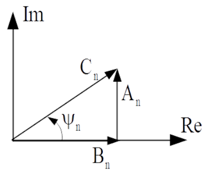
[latex]c(t) = c_0 + Im \left[|C_n|e^{j(n\omega_1 t + \psi_n)} \right] = c_0 + \sum_{n=1}^{\infty} |C_n| \sin( n\omega_1 t + \psi_n) \label{cc}\tag{1.57}[/latex]
[latex]c_0 = a_0 \label{c0}\tag{1.58}[/latex]
[latex]|C_n| = \sqrt{A_n^2 + B_n^2} \label{c}\tag{1.59}[/latex]
[latex]\psi_n = \arctan \left( \frac{A_n}{B_n} \right) \label{psi}\tag{1.60}[/latex]
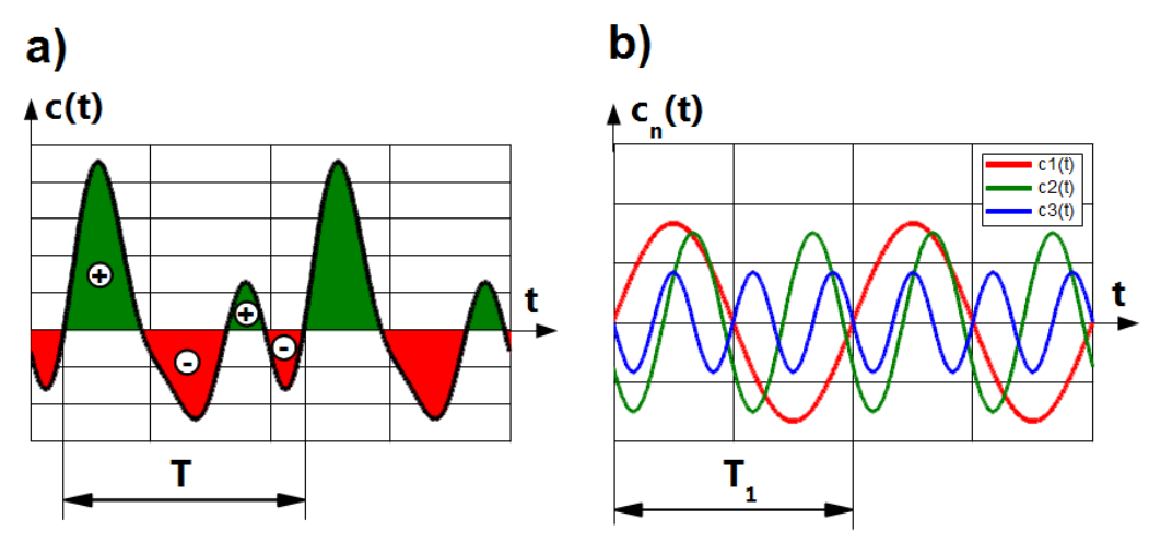
In Fig.1.24 an example of periodic function with constant component and harmonics [latex]n=1[/latex], [latex]n=2[/latex], [latex]n=3[/latex] is shown. Period [latex]T[/latex] of this function is identical with period [latex]T_1[/latex] of fundamental harmonic. It is general rule. Constant component is proportional to area below plot [latex]c(t)[/latex] (black curve in Fig.1.24 a)). This area above time axis has positive sign (red colour in Fig.1.24 a)) and negative below time axis (green colour Fig.1.24 a)).
Spectral density per frequency unit of a single event [latex]u(t)[/latex] is represented with the Fourier integral as follows
[latex]u(f) = \int_{-\infty}^{\infty} u(t) e^{-j2\pi f t} dt \label{Fourier_int}\tag{1.61}[/latex]
- It means serial resonance of the source and the load impedance by which the current is maximal and there is no reactive power commuting between the source and the load.↩︎
- Usually reference impedance is resistance ([latex]{\bf{Z}}_0 = 50 \Omega[/latex]).↩︎
- More frequently the term front time is used. Here the term crest time rationalizes assigning index “c” in symbol [latex]t_c[/latex]. Symbol [latex]t_f[/latex] is dedicated to fall time.↩︎