
4 Propagation of disturbances
There are four ways for disturbance to pass from the source to the victim, via:
- galvanic coupling,
- capacitive (electric) coupling,
- inductive (magnetic) coupling,
- wave coupling.
The first three accompany transmission of power or signals via conductors. It can proceed unsymmetrically or symmetrically.
Unsymmetrical transmission comes about when return conductor is common for more circuits and nonzero current as an overlay of currents of all circuits drives in the common return path. Three examples are shown in Fig.4.1. The return path can be identical with feeding lines or can differ with them.

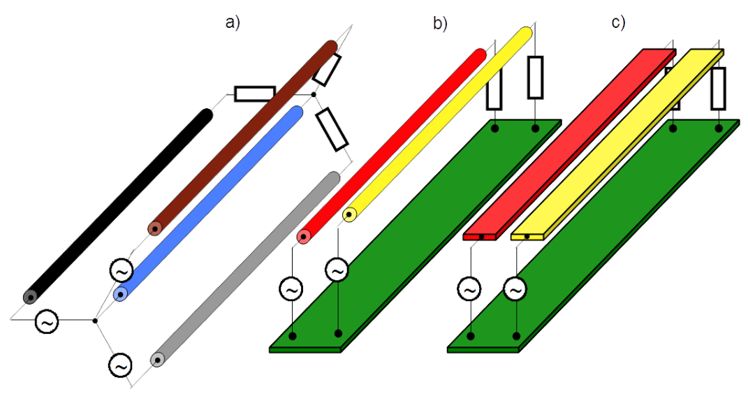
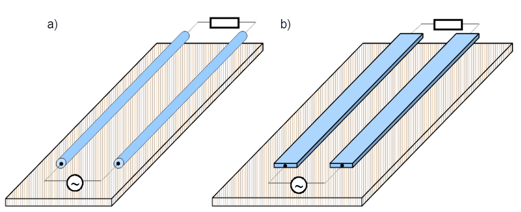
Symmetrical transmission is carried with a pair of identical conductors isolated from the surrounding. Examples are shown in Fig.4.2. There is always better or worse conducting layer beneath (striped plane) which builds the ground reference.

Unsymmetrical transmission is potentially accompanied with galvanic, capacitive and inductive coupling. Symmetrical transmission only with capacitive and inductive. They must be considered simultaneously. Here the phenomena will be presented separately in order to catch its essence. Such approach is violation of circuit theory, provide only one type of coupling is dominant, remaining negligible. It is case dependent.
Examples of unsymmetrical and symmetrical transmission
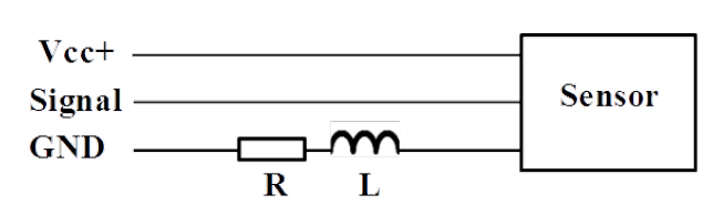
An example of unsymmetrical transmission is cabling of a sensor as shown in Fig.4.3 in which supply circuit [latex]V_{cc+}[/latex] and signal circuit have the same return path [latex]GND[/latex].

Another example is electrical installation in vehicles which very often is single ended. Return path is vehicle’s chassis.
Mind that three phase supply system shown in Fig.4.1a) with Neutral (blue line) as return path is an example of unsymmetrical transmission as soon as current is driven in the neutral line. One case common for house installation is presented below.
Low voltage AC power is delivered to a house as shown in Fig.[Lemp_1] in chapter [Thunderstorm]. Regulations forces to carry out the supply line between the transformer and the building input as the TN-C system [@IEC-60364-1]. It is four line supply system in which the Neutral line [latex]N[/latex] acts just as well as the Protective Earth line [latex]PE[/latex], therefore it is called [latex]PEN[/latex] line.
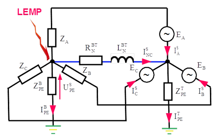
In Fig.4.4 electric circuit of the transformer with Line to Neutral EMF: [latex]E_A[/latex], [latex]E_B[/latex] and [latex]E_C[/latex] feeding the building with the four line system [latex]L_1[/latex], [latex]L_2[/latex], [latex]L_3[/latex] and [latex]PEN[/latex] is shown. [latex]Z_A[/latex], [latex]Z_B[/latex] and [latex]Z_C[/latex] represents impedances of the whole building installation seen from the feeding point of the building. [latex]Z_{PE}^B[/latex] and [latex]Z_{PE}^T[/latex] are earthing impedances of the star point of the building and the transformer respectively. By direct strike of the lightning electromagnetic pulse [latex]LEMP[/latex] in the external lightning protection system of the building the current is driven to the star point of the building where it is split as shown with the red arrows in Fig.4.4. The biggest part of the current drives to the Earth through earthing impedance of the building [latex]Z_{PE}^B[/latex] but due to the fact that between the building and the transformer there is common [latex]PEN[/latex] line, part of the current is driven as the surge in the whole installation inside the building and between the building and the transformer.
Usually there are more customers supplied from one transformer, as shown in Fig.[Lemp_1]. Due to galvanic connection of all of them with the star point of the transformer, all customers experiences the surge with different degree.
More resistive against surges would be the TN-S system [@IEC-60364-1]. It is five line supply system which has separate the Neutral [latex]N[/latex] and the Protective Earth [latex]PE[/latex] line.
Example of symmetrical transmission can be:
- power or signal cables of house installation layouted in the walls, ceilings or floors,
- cables layouted on the mounting plate in the control cabinet of a system,
- signal paths on the printed circuit board.
Galvanic coupling
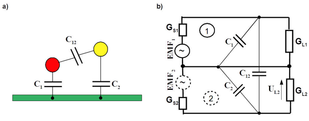
Galvanic coupling is illustrated in Fig.4.5 with very simple situation. There is a circuit composed of two meshes. In mesh 1 there is a source of power or a signal with electromotive force [latex]EMF_1[/latex] and internal resistance [latex]R_{S1}[/latex] and load [latex]R_{L1}[/latex]. The second with [latex]EMF_2[/latex] and [latex]R_{L2}[/latex]. Intension is to deliver electric power or signal from [latex]EMF_1[/latex] to [latex]R_{L1}[/latex] and from [latex]EMF_2[/latex] to [latex]R_{L2}[/latex]. However for some reason the two meshes have common return path represented with [latex]R_{GND}[/latex] and [latex]L_{GND}[/latex] which build the impedance [latex]Z_{GND}=R_{GND} + j \omega L_{GND}[/latex].

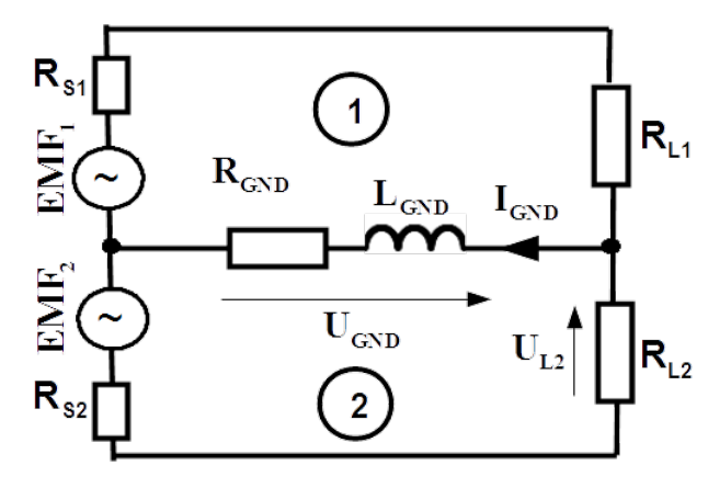
Each loop has self-inductance. It is composed of external inductance depending on wires layout and consequently on the area of the loop they build. Internal inductance of wires from which the loops are built also contribute to the total inductance. Obviously inductance must be assigned to the mesh but it is justified to extract the internal inductance of the common return path [latex]L_{GND}[/latex] as shown in Fig.4.5 because it is the attribute of the return path. External inductances of both meshes and internal inductances of feeding wires are disregarded as declared earlier.
Voltage [latex]U_{GND}[/latex] across the common return path represented with impedance [latex]Z_{GND}[/latex] is as follows
[latex]U_{GND} = -\frac{ \frac{EMF_1}{RS1+RL1} + \frac{EMF_2}{RS2+RL2} } { \frac{1}{R_{S1}+R_{L1}} + \frac{1}{R_{S2}+R_{L2}} + \frac{1}{Z_{GND}}} \label{U_GND}\tag{4.1}[/latex]
Voltage [latex]U_{L2}[/latex] across the load resistance [latex]R_{L2}[/latex] in mesh 2 is as follows
[latex]U_{L2} = \frac{ R_{L2}} {R_{S2}+R_{L2}} \left( EMF_2 - U_{GND} \right) \label{U_L2}\tag{4.2}[/latex]
Electromotive force [latex]EMF_1[/latex] contributes to the voltage [latex]U_{L2}[/latex] across the load of mesh 2 as follows
[latex]U_{L2}^{EMF_1} = - \frac{ R_{L2} \cdot EMF_1} { (R_{S1}+R_{L1}) (R_{S2}+R_{L2}) \left( \frac{1}{R_{S1}+R_{L1}} + \frac{1}{R_{S2}+R_{L2}} + \frac{1}{Z_{GND}} \right) } \label{U_2}\tag{4.3}[/latex]
The common return path causes unintentional contribution of [latex]EMF_1[/latex] to voltage across [latex]R_{L2}[/latex] and vice versa, via galvanic coupling.
Obviously, coupled voltage [latex]U_{L2}^{EMF_1}[/latex] would disappear by zero voltage [latex]U_{GND}[/latex] across the common return path. It can happen in two cases:
- by zero impedance of the return path [latex]Z_{GND}=0\Omega[/latex]. That is unrealistic to achieve.
- by total symmetry of the meshes i.e. if electromotive forces have the same amplitude and opposite phases. Moreover impedances of both paths are the same. In most cases it does not have sense by energy as well signal transmission.
Moreover perfect galvanic decoupling will happen with replacement of electromotive forces [latex]EMF_1[/latex] and [latex]EMF_2[/latex] with current sources. By power transportation it is hardly to imagine but transmission of current signals is used very often for that reason.
Intensity of galvanic coupling rises with increased impedance of the return path. By [latex]Z_{GND}[/latex] tending to infinity, [latex]I_{GND}[/latex] tends to zero and coupled voltage [latex]U_{L2}[/latex] approaches maximum expressed with the formula below
[latex]U_{L2_{MAX}}^{EMF_1} = \lim_{Z_{GND} \rightarrow \infty} U_{L2}^{EMF_1} = \frac{ R_{L2} \cdot EMF_1} {R_{S1}+R_{S2}+R_{L1}+R_{L2} } \label{U_2max}\tag{4.4}[/latex]
As galvanic coupling rises with increased internal impedance [latex]Z_{GND}[/latex] of the common return path it is valuable to investigate frequency dependence of impedance [latex]Z_{GND}[/latex]. This impedance depends on the shape of the cross section of the conductor. Considered are two cases for: round wire and rectangle cross section.
Internal impedance of round wire
Considered is idealized case of infinitely long strait wire with circular cross-section with radius [latex]r[/latex] placed in free space in order to neglect proximity effects. Segment of such wire with length [latex]l[/latex] is shown in Fig.4.6a).

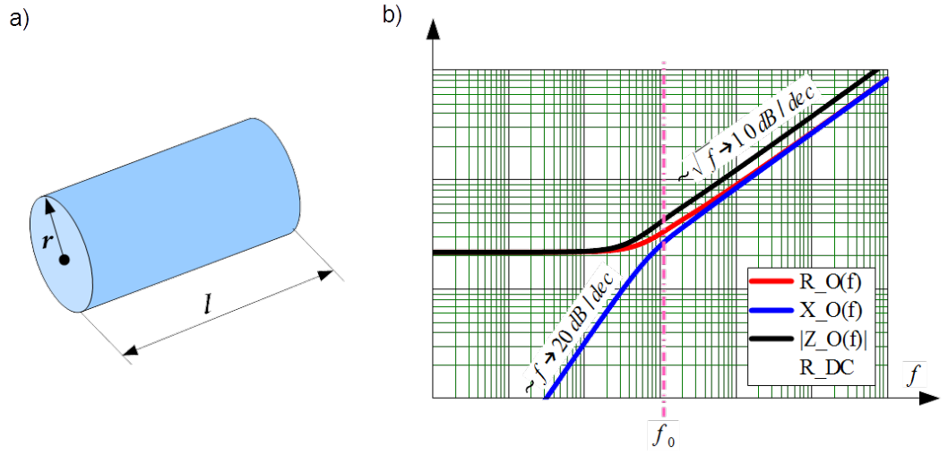
Impedance of such wire per unit length yields
[latex]Z(f) = \frac{k(f)}{2 \pi r \sigma} \frac{J_0[k(f)r]}{J_1[k(f)r]} \label{Z_f}\tag{4.5}[/latex]
where [latex]J_0[k(f)r][/latex] and [latex]J_1[k(f)r][/latex] are Bessel’s functions of zero and first order, [latex]\sigma[/latex] and [latex]\mu[/latex] is conductivity and magnetic permeability of wire material respectively and [latex]k(f)[/latex] is the wave number in the wire material
[latex]k(f) = \frac{1-j}{\delta (f)} \label{k_f}\tag{4.6}[/latex]
[latex]\delta(f)[/latex] is called the skin depth
[latex]\delta(f) = \sqrt{\frac{2}{\omega \mu \sigma}} \label{delta}\tag{4.7}[/latex]
which expresses depth in which current density is [latex]e[/latex] times smaller than on the surface of the wire, where [latex]e[/latex] is Euler’s number. To be precise it is valid for plane wave facing infinite conducting medium oriented perpendicularly to the direction of the wave propagation.
By low frequencies the real part of impedance [latex]Z(f)[/latex], Eq.(4.5) is nothing else but DC resistance of the round wire
[latex]R_{LF} = \frac{1}{\pi \sigma r^2} \label{R_LF}\tag{4.8}[/latex]
By high frequencies the real part of impedance [latex]Z(f)[/latex], Eq.(4.5) can be solved as if the current flowed uniformly through a layer of thickness equal to skin depth [latex]\delta[/latex]. The effective cross-sectional area for driving the current would be then approximately equal to skin depth [latex]\delta[/latex] times the conductor’s circumference [latex]2r-\delta \approx 2r[/latex]. Thus HF resistance of round wire is approximately equal to DC resistance of a hollow tube with wall thickness [latex]2r-\delta \approx 2r[/latex] carrying direct current
[latex]R_{HF}(f) = \frac{1}{\pi \sigma [2r-\delta(f)]\delta(f)} \approx \frac{1}{2 \pi \sigma r \delta(f)} \label{R_HF}\tag{4.9}[/latex]
Static and low frequency inductance of the round wire, accompanying uniformly flowed current is independent on wire radius [latex]r[/latex] [@Clayton]
[latex]L_{DC} = \frac{\mu}{8 \pi } \label{L_DC}\tag{4.18}[/latex]
Thus the imaginary part of impedance [latex]Z(f)[/latex], Eq.(4.5) i.e. reactance [latex]X_{LF}(f)[/latex] in low frequencies depends linearly on frequency [latex]X_{LF}(f) = 2 \pi f L_{DC} \label{X_LF}\tag{4.11}[/latex]
By high frequencies reactance and resistance are equal [latex]X_{HF}(f) = R_{HF}(f)[/latex]. It can be explained with the plane electromagnetic wave penetrating good conducting medium. The wave impedance has then equal real and imaginary part.
Frequency dependence of the internal impedance of the round wire in double logarithmic scale is illustrated in Fig.4.6b). Breaking frequency [latex]f_0[/latex] marked there, which is border between low and high frequency regions can be established equating LF resistance and reactance
[latex]f_0 = \frac{4}{\pi \mu \sigma r^2} \label{f_0}\tag{4.12}[/latex]
Mind that low frequency reactance is proportional to frequency, therefore it is strait line with the slope [latex]20dB/dec[/latex], compare Eq.(4.11). The HF resistance and reactance are reciprocally proportional to the skin depth [latex]\delta(f)[/latex], see Eq.(4.9) therefore they increase proportionally to the square root of frequency. In other words they have slopes [latex]10dB/dec[/latex]. Module of high frequency impedance [latex]|Z_{GND}(f)|[/latex] is by factor [latex]\sqrt{2}[/latex] bigger than HF resistance or reactance, because they are equal one to another. In double logarithmic scale it is bigger about [latex]3dB[/latex].
Eq.(4.12) gives the hint how to keep impedance of the round wire small up to relatively high frequencies. The trick consists in keeping the radius [latex]r[/latex] of wire relatively small. It is done in so called HF litz-wire in which wire is composed of bundle of individually isolated strands, as shown in Fig.4.7.

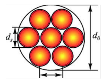
In such wire, in spite of the cross-section equal to sum of cross-sections of individual strains, the breaking frequency Eq.(4.12) is correlated with individual strain1.
Internal impedance of conductor with rectangular cross section
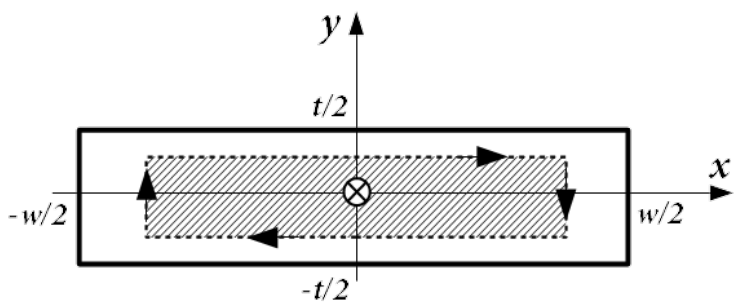
Considered is idealized case of infinitely long strait conductor with rectangular cross section with width [latex]w[/latex] and thickness [latex]t[/latex] placed in free space in order to neglect proximity effects. Segment of such wire with length [latex]l[/latex] is shown in Fig.4.8a).
Unlike by round wire no analytical formula exist for such conductor.
The low frequency resistance yields
[latex]R_{LF} = \frac{1}{\sigma w t} \label{R_LF_wt}\tag{4.13}[/latex]
By high frequencies resistance can be solved as by round wire i.e. as if the current flowed uniformly through a layer of thickness equal to skin depth [latex]\delta[/latex]. The effective cross-sectional area for driving the current would be then approximately equal to skin depth [latex]\delta[/latex] times the conductor’s circumference [latex]2 (w + t)[/latex]. Thus HF resistance of round wire is approximately equal to DC resistance of a hollow rectangular tube with wall thickness [latex]\delta[/latex] carrying direct current [@Clayton_MTL]
[latex]R_{HF}(f) = \frac{1}{2 \sigma \delta(f) (w+t)} \label{R_HF_wt}\tag{4.14}[/latex]

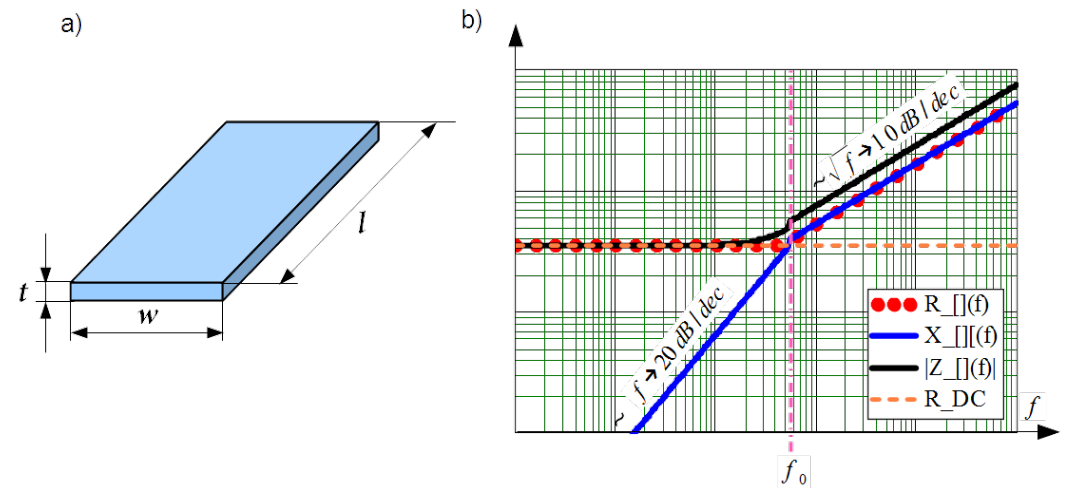
Prime to derivation of static and low frequency inductance of the conductor, distribution of magnetic field inside the conductor must be considered. If in the whole cross section uniformly distributed current [latex]I[/latex] is driven, then circulation of magnetic field along the rectangular circumference shown with dashed line in Fig.4.9 yields
[latex]2\cdot H_x(y) \cdot 2x + 2\cdot H_y(x) \cdot 2y = \frac{I}{wt } \cdot 4xy \label{HxHy}\tag{4.16}[/latex]
[latex]H_x(y) = \frac{I}{wt } \cdot y \label{HxHy}\tag{4.16}[/latex]
This is valid only if [latex]H_x(y)[/latex] is constant along the whole length of horizontal sides and contribution of circulation along vertical sides can be neglected. These rough simplification are justified provide [latex]w \gg t[/latex].

Internal inductance can be directly computed from energy relation by equating magnetic energy stored inside the conductor expressed with magnetic field strength [latex]\stackrel{\rightarrow}{H}(x,y)[/latex] to the same energy expressed with the internal inductance [latex]L_{DC}[/latex]
[latex]\frac{1}{2} L_{DC} I^2 = \frac{\mu}{2} \int_{S} |H(x,y)|^2 dS = \frac{\mu}{2} \cdot \frac{I^2}{w^2 t^2} \int_{-\frac{w}{2}}^{-\frac{w}{2}}dy \int_{-\frac{t}{2}}^{-\frac{t}{2}}x^2dx \label{Hx}\tag{4.17}[/latex]
Finally
[latex]L_{DC} = \frac{\mu}{12 } \cdot {t}{w} \label{L_DC}\tag{4.18}[/latex]
Breaking frequency [latex]f_0[/latex] can be established as by the round wire with equating LF resistance and reactance
[latex]f_0 = \frac{6}{\pi \mu \sigma t^2} \label{f_0_xy}\tag{4.19}[/latex]
Frequency dependence of the internal impedance of conductor with rectangle cross section in double logarithmic scale is illustrated in Fig.4.8b). Qualitatively it is identical with behavior of the round wire shown in Fig.4.6b).

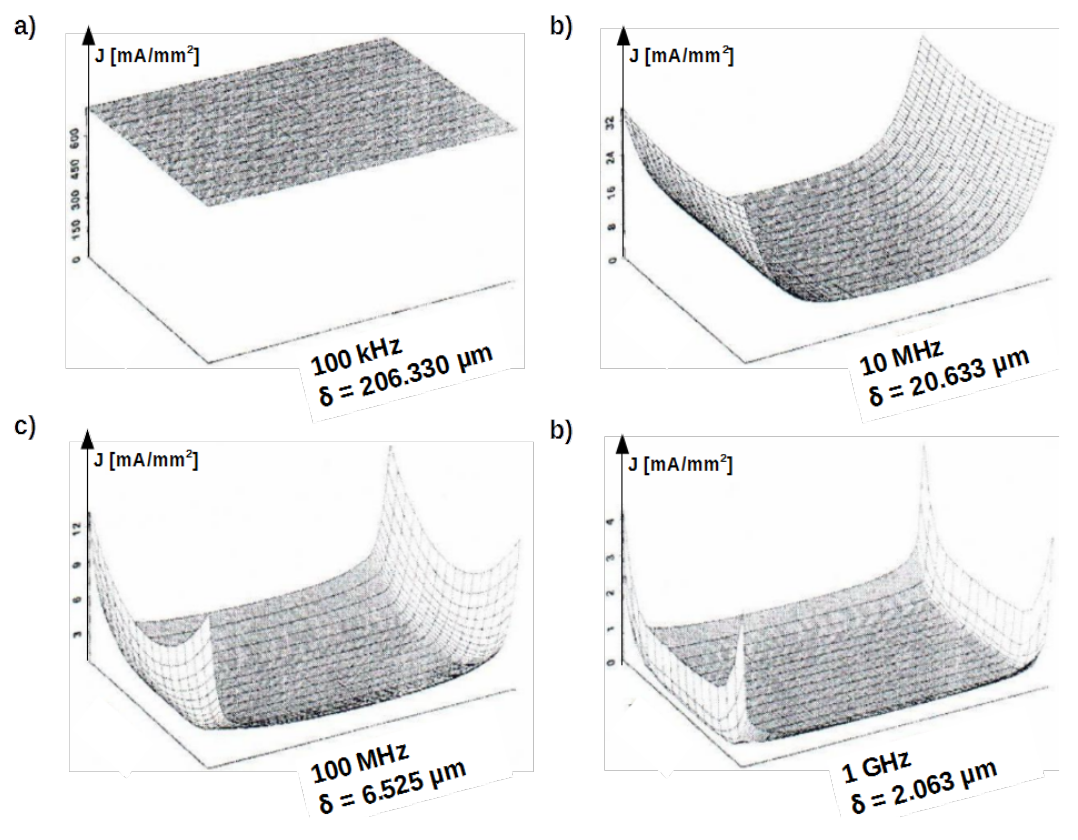
An example of distribution of current density in the rectangular conductor in frequency dependence, sourced from [@Clayton_MTL] is shown in Fig.4.10. Features notable in it are summarized below:
- current crowding toward the outer edge is remarkable only in direction for which the skin depth [latex]\delta(f)[/latex] is much smaller than the side of the rectangle,
- current which is the integral of current density [latex]J(x,y)[/latex] over the cross section surface is the smaller the bigger frequency is, because impedance of conductor rises,
- proportionality of the skin depth [latex]\delta(f)[/latex] to the square root of frequency [latex]\sqrt f[/latex] can be confirmed.
Precedence of rectangular conductor over round wire
It is desired to compare impedance [latex]Z_{GND}[/latex] of the common path for different shape of the cross section because as presented in previous sections it is shape dependent.
Breaking frequency is the upper bound of the frequency by which internal impedance is kept relatively deep i.e. impedance is only slightly bigger than DC resistance. Comparison of Eq.(4.12) and Eq.(4.19) shows unequivocally that [latex]f_0[/latex] is much bigger for conductor with rectangle cross section. Indeed in case of rectangle cross section the number in numerator is bigger than by round wire, 6 instead of 4 but crucial is thickness in square in denominator which by [latex]w \gg t[/latex] is much smaller than square of radius [latex]r[/latex] in case of round wire. By comparison of HF litz-wire and rectangle conductor the break frequencies can be similar but costs of HF litz-wire exceeds pretty costs of ordinary solid conductor.
This rationalises precedence of rectangular conductor over round wire. The wider conductor with rectangle cross section by unchanged thickness the smaller low frequency resistance [latex]R_{LF}[/latex]. Therefore as shown in Fig.[Unsym_line]c) by double layers’ PCBs the return path are as wide as practical and by multilayers’ PCBs separate layer or even more layers are dedicated to the return paths.
Electric (capacitive) and magnetic (inductive) coupling
Capacitive coupling

Total voltage across load conductance [latex]G_{L2}[/latex] yields
[latex]U_{L2_{total}} = \frac{ G_{S2}(G_{L1} + G_{S1} + Y_1 + Y_{12}) \cdot EMF_2 + G_{S1} Y_{12} \cdot EMF_1} { (G_{L1}+G_{S1} + Y_1) (G_{L2}+G_{S2} + Y_2) + Y_{12} (G_{L1}+G_{L2} + G_{S1} + G_{S2} +Y_1 + Y_2) } \label{U_2C_tot}\tag{4.20}[/latex]
where [latex]Y = j \omega C[/latex] is admittance of a capacitor
Electromotive force [latex]EMF_1[/latex] contributes to the voltage [latex]U_{L2}[/latex] across the load conductance [latex]G_{L2}[/latex] of mesh 2 as follows
[latex]U_{L2} = \frac{ G_{S1} Y_{12} \cdot EMF_1} { (G_{L1}+G_{S1} + Y_1) (G_{L2}+G_{S2} + Y_2) + Y_{12} (G_{L1}+G_{L2} + G_{S1} + G_{S2} +Y_1 + Y_2) } \label{U_2C}\tag{4.21}[/latex]
Obviously, coupled voltage [latex]U_{L2}[/latex] would be zero by zero mutual capacitance [latex]C_{12}[/latex], [latex]Y_{12}=0 \frac{1}{\Omega}[/latex]. That is unrealistic. There exist always capacitance between two metallic objects as signal or power lines. Even replacement of electromotive forces [latex]EMF_1[/latex] and [latex]EMF_2[/latex] with current sources does not liberate from capacitive coupling.
Inductive coupling
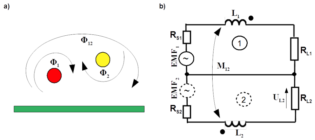
Total voltage across load resistance [latex]R_{L2}[/latex] yields
[latex]U_{L2_{total}} = \frac{R_{L2}}{R_{L2}+ R_{S2} + Z_2+Z_{12}} \left[EMF_2 - \frac{ \frac{EMF_1}{R_{L1} + R_{S1} + Z_1+Z_{12}} + \frac{EMF_2}{R_{L2} + R_{S2} + Z_2+Z_{12}}} {\frac{1}{R_{L1} + R_{S1} + Z_1+Z_{12}} + {\frac{1}{R_{L2} + R_{S2} + Z_2+Z_{12}} - \frac{1}{Z_{12}} }} \right] \label{U_2L_tot}\tag{4.22}[/latex]
where [latex]Z_1 = j \omega L_1[/latex] and [latex]Z_2 = j \omega L_2[/latex] are impedances of self inductances [latex]L_1[/latex] and [latex]L_2[/latex] respectively. [latex]Z_{12} = j \omega M_{12}[/latex] is impedance of a mutual inductance [latex]M_{12}[/latex]. It depends on self inductances as follows [latex]M_{12} = k \sqrt{L_1 L_2}[/latex] where [latex]0Dependence of capacitance and external inductance on cross section’s shape
 [caption id="attachment_174" align="aligncenter" width="633"]
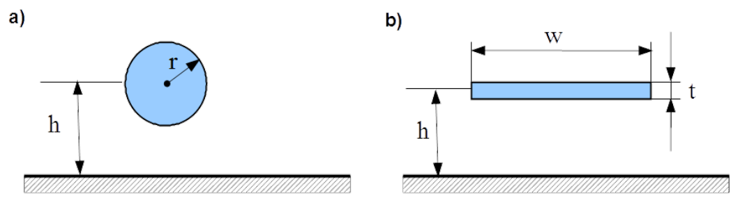 Figure 4.13: Illustration for consideration of capacitance and external inductance.[/caption]
Capacitance per unit length of a infinitely long strait wire with circular cross section, layouted in air parallel to infinite conducting plane, as shown in Fig.4.13a) yields [@Clayton] [latex]C_{\bigcirc} = \frac{2\pi\varepsilon_0}{\operatorname{ar\,cosh} \left(\frac{ h}{r} \right)} \label{C_r}\tag{4.24}[/latex]
where [latex]\operatorname{ar\,cosh} (x) = \ln \left[ \sqrt{x^2-1} + x \right] \approx \ln(2x)[/latex] for [latex]x \gg 1[/latex]. Therefore for a wire that is sufficiently far from the conducting plane, [latex]h \gg r[/latex] this simplifies to
[latex]\begin{array} {ll} C_{\bigcirc} \approx \frac{2\pi\varepsilon_0}{\ln \left(\frac{ 2h}{r} \right)} & \text{for}~~h \gg r \end{array} \label{C_r_approx}\tag{4.25}[/latex]
As explained in chapter [El size], wave propagates along a transmission line if it is electrically long. Velocity of propagation is the quantity that binds parameters [latex]\mu[/latex] and [latex]\varepsilon[/latex] of the surrounding medium with per length parameters [latex]L[/latex] and [latex]C[/latex] of the transmission line. On one side it is given as in Eq.([v_propagation]), on the other side as [latex]v = \frac{1}{\sqrt{LC}}[/latex]. Therefore by homogeneous surrounding of transmission line holds
[latex]L \: C = \mu \: \varepsilon \label{LC}\tag{4.26}[/latex]
This straightforwardly leads to formulas for external inductance of the round wire
[latex]L_{\bigcirc}^{EXT} = \frac{\mu_0}{2\pi} \operatorname{ar\,cosh} \left(\frac{ h}{r} \right) \label{L_r}\tag{4.27}[/latex]
[latex]\begin{array} {ll} L_{\bigcirc}^{EXT} \approx \frac{\mu_0}{2\pi} \ln{\left (\frac{2h}{r} \right)} & \text{for}~~h \gg r \end{array} \label{L_r_approx}\tag{4.28}[/latex]
There exist no general analytical formula for parameters of conductor with rectangular cross section. Cited here is approximate relation for the case shown in Fig.4.13b), according to [@Clayton], assuming zero thickness of conductor
[latex]\begin{array} {ll} C_{\framebox[0.15in]{}} \approx \varepsilon_0 \left[ \frac{w}{h} + 1.393 + 0.667 \ln{\left (\frac{w}{h} + 1.444 \right)} \right] & \text{for}~~w \geq h \end{array} \label{C_rect}\tag{4.29}[/latex]
[latex]\begin{array} {ll} L_{\framebox[0.15in]{}}^{EXT} \approx \frac{ \mu_0}{ \frac{w}{h} + 1.393 + 0.667 \ln{\left (\frac{w}{h} + 1.444 \right)}} & \text{for}~~w \geq h \end{array} \label{L_rect}\tag{4.30}[/latex]
Capacitance of the round wire with [latex]2.5mm^2[/latex] cross section area i.e. with radius [latex]=0.892mm[/latex] layouted [latex]h=1cm[/latex] above ground plane, according to Eq.(4.25) amounts to [latex]C_{\bigcirc}=17.89pF/m[/latex]. Rectangular conductor with the same cross section area and longer size [latex]w=2cm[/latex] has shorter size [latex]t=0.125mm[/latex]2. According to Eq.(4.29) its capacitance is [latex]C_{\framebox[0.15in]{}}=37.35 pF/m[/latex].
Analogue is with external inductance. By the same geometry relations, according to Eq.(4.28) external inductance of the round wire amounts to [latex]L_{\bigcirc}^{EXT}=0.622 \mu H/m[/latex] and by rectangular conductor is [latex]L_{\framebox[0.15in]{}}^{EXT}=0.298 \mu H/m[/latex], according to Eq.(4.30).
In numerical example above capacitance/external inductance is smaller/ bigger for a round wire/rectangular conductor. This example is realistic and the relation can be generalized. Rationale of it is rooted in the Euclidean geometry. It is taught there, that from all plane figures, the circle has the smallest ratio of circumference to surface area.
Let us compare capacitances. The Gauss’s flux theorem is a law relating the distribution of electric field to charges originating it. The electric flux through any hypothetical closed surface [latex]S[/latex] is equal to the net electric charge [latex]Q[/latex] within that closed surface [latex]\varepsilon_0 \oiint_S \overrightarrow{E}\cdot \overrightarrow{dS} = \sum Q[/latex]. For infinite strait conductor the electric flux can be calculated through the surface per unit length and therefore it is reduced to the integral along arbitrary closed loop enclosing the conductor.
Let us compare round wire and rectangular conductor with the same surface area, layouted on the same height [latex]h[/latex] above the ground plane. For round wire the integration path is shorter than for rectangular conductor, due to ratio of circumference to area. Therefore if in both cases net charge is the same, electric field strength distributed around rectangular conductor is smaller.
Voltage across conductor and the ground plane is given by the line integral of electric field along arbitrary path between them [latex]U = \int_l \overrightarrow{E}\cdot \overrightarrow{dl}[/latex]. Consequently it is smaller in case of rectangular conductor. Capacitance is ratio of free charge on the conductor or the ground plane to voltage necessary for gathering this amount of charge [latex]C=Q/U[/latex]. Conclusion is that, for gathering particular net charge less voltage is needed in case of rectangular conductor than of round wire. Finally, capacitance of rectangular conductor is bigger than of round wire.
Similarly can be proceeded by comparing external inductances. The Ampere’s circular low relates the distribution of magnetic field strength to current causing it. The line integral of magnetic field strength [latex]\overrightarrow{H}[/latex] along any hypothetical closed loop [latex]l[/latex] is equal to the net current [latex]I[/latex] enclosed in this loop [latex]\oint_l \overrightarrow{H}\cdot \overrightarrow{dl} = \sum I[/latex].
Let us compare round wire and rectangular conductor with the same surface area, layouted on the same height [latex]h[/latex] above the ground plane. For round wire the integration path is shorter than for rectangular conductor, due to ratio of circumference to area. Therefore if in both cases enclosed net current is the same, magnetic field strength distributed around rectangular conductor is smaller.
Magnetic flux through any hypothetical surface built by the loop driving current [latex]I[/latex] is given by [latex]\Phi = \mu_0 \oiint_S \overrightarrow{H}\cdot \overrightarrow{dS}[/latex]. For infinite loop composed of round wire or rectangular conductor, load in infinity and the ground plane as return path, only flux per unit length makes sense. It is smaller in case of rectangular conductor due to smaller field strength. Inductance is ratio of magnetic flux to current necessary for generating it [latex]L=\Phi/I[/latex]. It means that, by driving the same particular net current less flux is generated in case of rectangular conductor than of round wire. Finally, inductance of rectangular conductor is smaller than of round wire.
This statement can be rationalised alternatively starting with comparison of capacitances along with conclusion from Eq.(4.26).
Notice, that capacitance/external inductance of the round wire rises/decays slower with increased radius [latex]r[/latex] than capacitance/external inductance of the rectangular conductor with its width [latex]w[/latex]. In the first case the change is compressed because radius is argument of natural logarithm. In the second case, dependence on width [latex]w[/latex] is direct.
Capacitive and inductive coupling by symmetrical transmission
Up to now only unsymmetrical transmission was covered. The only message concerning symmetrical transmission discussed here is the size of zone surrounding transmission line in which risk of capacitive or inductive coupling exist.

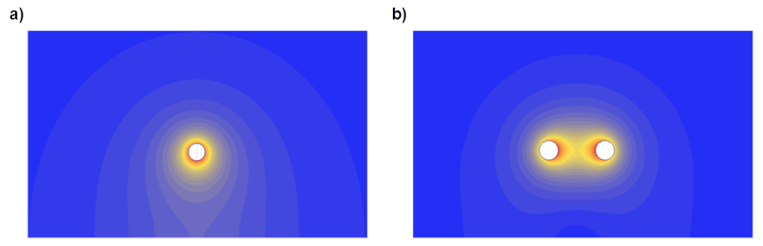
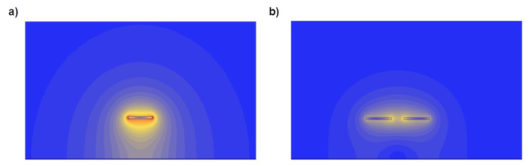
In Fig.4.14 distribution of module of electric field strength around unsymmeric and symmetric transmission line with round wire is illustrated. The same voltage is applied and spectrum of colours has the same scale in both cases.
Evidently the zone polluted with the electric field in case of symmetrical transmission is smaller. Module of electric field strength by symmetrical line decays stronger versus distance from the line in horizontal as well vertical direction. Rationale for it is the fact that space between feeding and return line in case of symmetrical transmission is much smaller than in case of unsymmetrical transmission. Fields outside the line cancel one another. As a consequence of it, zone with practically total cancellation of field is closer to the line in the case of symmetrical transmission.
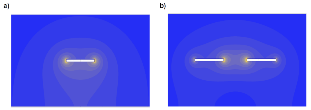
The same can be concluded for unsymmetrical and symmetrical lines build of conductors with rectangular cross sections as shown in Fig.4.15.
In Fig.4.16 distribution of module of magnetic field strength around unsymmeric and symmetric transmission line with round wire is illustrated. The same current is driven and spectrum of colours has the same scale in both cases.
Evidently the zone polluted with the magnetic field in case of symmetrical transmission is smaller.


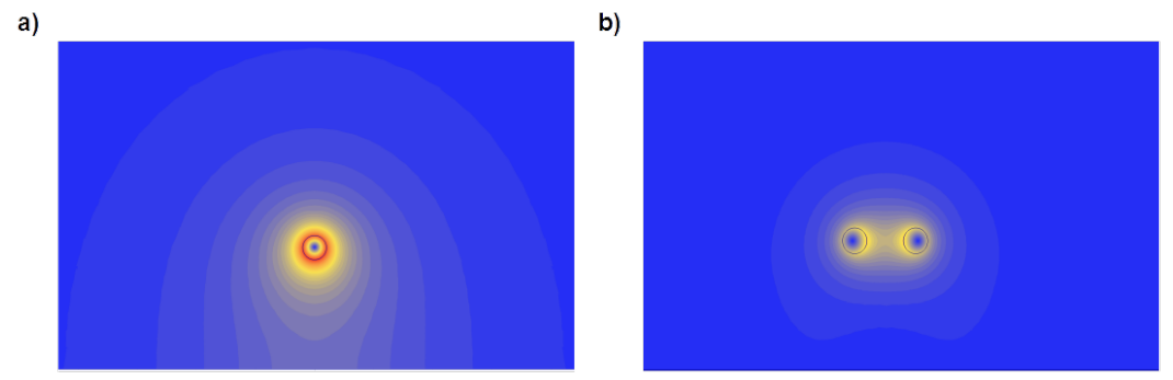

The same can be concluded for unsymmetrical and symmetrical lines build of conductors with rectangular cross sections as shown in Fig.4.17.
Transverse to longitudinal conversion
Equivalent scheme of symmetric transmission is shown in Fig.4.18. Energy or signal should be delivered from the source [latex]EMF[/latex] with internal resistance [latex]R_S[/latex] to the load [latex]R_L[/latex] via symmetrical line. This line is layouted above the ground. Each line i.e. feeding: 1-3 and return: 2-4 has parasitic capacitance related to the ground. They are represented with capacitances [latex]C_{10}[/latex] and [latex]C_{20}[/latex] by the source and [latex]C_{35}[/latex] and [latex]C_{45}[/latex] by the load. There are also parasitic capacitances of one to another line. They are represented with capacitances [latex]C_{12}[/latex] by the source and [latex]C_{34}[/latex] by the load. Moreover each line builds inductance represented with [latex]L_{13}[/latex] and [latex]L_{24}[/latex].
Symmetric transmission means that parasitic parameters are in equilibrium consisted in following identities [latex]\begin{array} {rcl} C_{10} = C_{20} \nonumber \\ C_{35} = C_{45} \nonumber \\ L_{13} = L_{24} \nonumber \end{array}[/latex]
In such situation [latex]U_{50} = 0[/latex]. Transmission line is perfectly balanced.

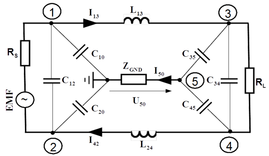
Electromotive force [latex]EMF[/latex], which is oriented crosswise to the direction of transmission generates voltage [latex]U_{50}[/latex] along direction of transmission only if the circuit is out balance.
Ratio of transverse electromotive force [latex]EMF[/latex] to longitudinal voltage [latex]U_{50}[/latex]
[latex]\begin{array} {rcl} L_{TC} & = & \frac{EMF}{U_{50}} \\ L_{TC(dB)} & = & 20 \log \left( \frac{EMF}{U_{50}} \right) \end{array} \label{TCL}\tag{4.35}[/latex]
is called loss of transverse (to longitudinal) conversion, alternatively Transverse Conversion Loss TCL. It is used for rating deviation from the ideal balance by symmetrical transmission. By approaching perfect equilibrium, [latex]L_{TC}[/latex] tends to infinity.
There are two reasons for transverse conversion to be undesired: deterioration of integrity of transmitted signal and enlargement of the zone around the line polluted with the electromagnetic field, similarly as by unsymmetrical transmission.
Decomposition of currents into common and differential mode
In this subsection currents in the transmission line shown in Fig.4.18 will be derived. For suppressing complexity of the formulas, source resistance [latex]R_S[/latex] will be omitted.
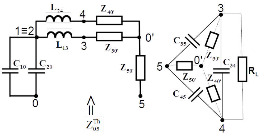
Voltage [latex]U_{50}[/latex] unequal to zero means current [latex]I_{50}[/latex] driven through the ground impedance [latex]Z_{GND}[/latex]. It can be calculated with the Thevenin’s Theorem. Open circuit voltage [latex]U_{50}^{Th}[/latex] by removing branch [latex]Z_{GND}[/latex] yields
[latex]U_{50}^{Th} = \frac{Y_{13} \left[Y_{34}(Y_{35} + Y_{45}) + Y_{35}(Y_{24} + Y_{45})\right] \cdot EMF} {(Y_{13} + Y_{24})\left[Y_{34}(Y_{35} + Y_{45}) + Y_{35} Y_{45} \right] + Y_{13} Y_{24}(Y_{35} + Y_{45})} - \frac{Y_{10}\cdot EMF}{Y_{10} + Y_{20}} \label{U50}\tag{4.36}[/latex]
where [latex]Y_{34} = \frac{R_L + \frac{1}{j\omega C_{34}}}{R_L \frac{1}{j\omega C_{34}}}[/latex]
For derivation of the Thevenin’s impedance seen between poles 5-0, transposition of triangle 3-4-5 to the star with the star node 0’ as shown in Fig.4.19 must be performed
[latex]\begin{array} {rcl} Z_{30'} = \frac{Z_{34} Z_{35}}{Z_{34} + Z_{35} + Z_{45}} \nonumber \\ \nonumber \\ Z_{40'} = \frac{Z_{34} Z_{45}}{Z_{34} + Z_{35} + Z_{45}} \nonumber \\ \nonumber \\ Z_{50'} = \frac{Z_{35} Z_{45}}{Z_{34} + Z_{35} + Z_{45}} \nonumber \end{array}[/latex]

Current [latex]I_{50}[/latex] driven through the ground impedance [latex]Z_{GND}[/latex] is called common mode current [latex]I^{CM}[/latex]. It yields
[latex]I^{CM} = I_{50} = \frac{U_{50}^{Th}} {Z_{50}^{Th} + Z_{GND}} \label{I50}\tag{4.38}[/latex]
In node 0 it is split to current [latex]I_{13}^{CM}[/latex] and [latex]I_{24}^{CM}[/latex] driven in line 1-3 and 2-4 respectively. Ratio of currents [latex]I_{13}^{CM}[/latex] and [latex]I_{24}^{CM}[/latex] depends on relation between impedances of paths 0-1-3-5 and 0-2-4-5.
Along with the common mode component the differential mode current [latex]I^{DM}[/latex] is driven in the feeding and return line.
It can be calculated after removing branch with the ground impedance [latex]Z_{GND}[/latex]
[latex]I^{DM} = I_{50} = \frac{EMF} {Z_{13} + Z_{24} + \frac{(Z_{35} + Z_{45}) Z_{34}}{Z_{35} + Z_{45} + Z_{34}}} \label{IDM}\tag{4.39}[/latex]
Finally actual currents in the transmission lines expressed with the common and differential components yields
[latex]\begin{array} {rcl} I_{13} & = & I^{DM} + I_{13}^{CM} \\ \\ I_{42} & = & I^{DM} - I_{24}^{CM} \end{array}[/latex]
Calculation of capacitances [latex]C_{10}[/latex], [latex]C_{20}[/latex] and [latex]C_{12}[/latex] as well [latex]C_{35}[/latex], [latex]C_{45}[/latex] and [latex]C_{34}[/latex] can be done only numerically because both triple of capacitors are linked. Any change of one of them causes changes of the rest.
The same concerns inductances. Notice that [latex]L_{13}[/latex] is serial connection of two inductances because line 1-3 is part of the loop 1-3-5-0 and 1-3-4-2.
Wave coupling
Radiated waves
Idealized entities as elementary radiators
- Isotropic antenna. It is omni directional radiator. In other words it radiates the same power in all directions.
- Electric (Hertzian) dipole. Imagine electrically short, infinitesimally thin strait conducting segment carrying a current represented with the phasor [latex]\bf{I}[/latex] that is assumed to be constant (as to magnitude and phase) at all points along the segment. If the segment length [latex]l[/latex] tends to zero whereas the current [latex]\bf{I}[/latex] infinitely growths so that the quantity [latex]{\bf{p}} = l{\bf{I}}[/latex] remains finite and constant, then this product constitutes magnitude of the vector called the dipole moment. Its direction is along the segment and the sense according to the current direction [latex]\overrightarrow{1}_l[/latex]
[latex]\overrightarrow{\bf{p}} = \lim \limits_{l \to 0, I \to \infty} (l{\bf{I}}) \overrightarrow{1}_l \label{p_dipole}\tag{4.41}[/latex]
- Magnetic (Fitzgeraldian) dipole. Imagine electrically small, infinitesimally thin ring with azimuthal current [latex]\bf{I}[/latex] flowing in it which does not depend on the angle. If the ring radius [latex]a[/latex] tends to zero whereas the current [latex]\bf{I}[/latex] infinitely growths so that the product of the ring area and current [latex]{\bf{m}} = \pi a^2 {\bf{I}}[/latex] remains finite and constant, then this product constitutes magnitude of the vector called the dipole moment. Its direction is orthogonal to the plane of the ring and the sense results from the vector product of unit radius vector [latex]\overrightarrow{1}_r[/latex] and unit current density vector [latex]\overrightarrow{1}_j[/latex]
[latex]\overrightarrow{\bf{m}} = \lim \limits_{ \pi a^2 \to 0, I \to \infty} (\pi a^2 {\bf{I}}) \overrightarrow{1}_r \times \overrightarrow{1}_j \label{m_dipole}\tag{4.42}[/latex]
All these entities are lossless. None of them exist in reality but they are useful in understanding the antenna theory including unintentional antennas such as cables connected to the EUT.

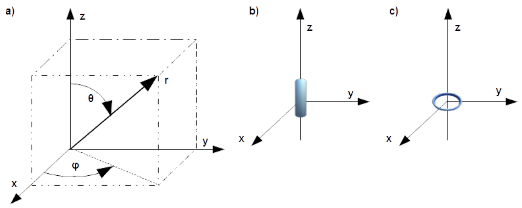
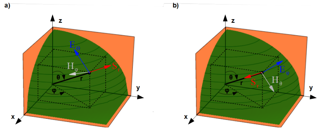
The best way of describing the 3D fields generated by dipoles is the spherical system of co-ordinates in which the spacial position of the point under interest is described with three following numbers: [latex]r, \theta, \varphi[/latex], as shown in Fig.4.20a). The radius [latex]r[/latex] is distance from the origin of the co-ordinates system, [latex]\theta[/latex] elevation angle between the [latex]z[/latex] axis and radius [latex]r[/latex], [latex]\varphi[/latex] is the azimuthal angle between [latex]x[/latex] axis and projection of the radius [latex]r[/latex] on the [latex]x0y[/latex] plane.
Components of the electric field strength of the electric dipole oriented as shown in Fig.4.20b), according to [@Clayton] are as follows
[latex]{\bf{E}}_r (r,\theta)= \frac{{\bf{p}}_z Z_0 \beta_0^2} {2 \pi} \cos{(\theta)} \left( \frac{1}{\beta_0^2 r^2} -j \frac{1}{\beta_0^3 r^3} \right) e^{-j\beta_0 r} \label{eE_r} \tag{4.43}[/latex]
[latex]{\bf{E}}_\theta (r,\theta)= \frac{{\bf{p}}_z Z_0 \beta_0^2} {4 \pi} \sin{(\theta)} \left( j \frac{1}{\beta_0 r} + \frac{1} { \beta_0^2 r^2} -j \frac{1}{\beta_0^3 r^3} \right) e^{-j\beta_0 r} \label{eE_theta} \tag{4.44}[/latex]
[latex]{\bf{E_\varphi}}= 0 \label{eE_phi} \tag{4.45}[/latex]
and of magnetic field strength
[latex]{\bf{H}}_r= 0 \label{eH_r} \tag{4.46}[/latex]
[latex]{\bf{H}}_\theta = 0 \label{eH_theta} \tag{4.47}[/latex]
[latex]{\bf{H}}_\varphi(r,\theta)= \frac{{\bf{p}}_z \beta_0^2} {4 \pi} \sin{(\theta)} \left( j\frac{1}{\beta_0 r} + \frac{1}{\beta_0^2 r^2} \right) e^{-j\beta_0 r} \label{eH_phi} \tag{4.48}[/latex]
where [latex]Z_0[/latex] is the intrinsic impedance of the medium in which the dipole is placed. It depends on the magnetic and dielectric constants [latex]\mu_0[/latex] and [latex]\epsilon_0[/latex] of the medium as follows
[latex]Z_0 = \sqrt{\frac{\mu_0}{\epsilon_0}} \label{Z_0}\tag{4.49}[/latex]
and [latex]\beta_0[/latex] is the phase constant of the wave expressed with the formula
[latex]\beta_0 = \omega \sqrt{\mu_0 \epsilon_0} = \frac{2 \pi}{\lambda_0} \label{beta}\tag{4.50}[/latex]
where [latex]\omega[/latex] is angular frequency of the propagated wave and [latex]\lambda_0[/latex] is the wave length.
Far away from the electric dipole, regardless of direction disappears dependence of electric field on the second and the third power of radius [latex]r[/latex], refer to Eqs. (4.43) and (4.44) and dependence of [latex]{\bf{H}}_ {\varphi}[/latex] component of magnetic field on the second power of radius [latex]r[/latex], refer to Eq. (4.48). Solely summands reciprocally proportional to the distance [latex]r[/latex] remains.
In the immediate vicinity of the electric dipole dominant is dependence of electric field on the third power of radius [latex]r[/latex], refer to Eqs. (4.43), (4.44). Zone within such solid is the near field zone. Magnetic field [latex]{\bf{H}}_{\varphi}[/latex] does not exist in it because it does not possess summand with radius [latex]r[/latex] in the third power. Emerges only electric field distributed as in static case. Therefore another name of the zone is the static zone.
Between the near field and the far field zone there is the buffer called the reactive zone.
Components of the electric field strength of the magnetic dipole oriented as shown in Fig.4.20c), according to [@Clayton] are as follows
[latex]{\bf{E}}_r = 0 \label{mE_r} \tag{4.51}[/latex]
[latex]{\bf{E}}_\theta = 0 \label{mE_theta} \tag{4.52}[/latex]
[latex]{\bf{E}}_\varphi (r,\theta)=-j \frac{ {\bf{m}}_z \omega \mu_0 \beta_0^2 } {4 \pi} \sin{(\theta)} \left( j\frac{1}{\beta_0 r} + \frac{1}{\beta_0^2 r^2} \right) e^{-j\beta_0 r} \label{mE_phi} \tag{4.53}[/latex]
and of magnetic field strength
[latex]{\bf{H}}_r (r,\theta)= j \frac{{\bf{m}}_z \omega \mu_0 \beta_0^2} {2 \pi Z_0 } \cos{(\theta)} \left( \frac{1}{\beta_0^2 r^2} -j \frac{1}{\beta_0^3 r^3} \right) e^{-j\beta_0 r} \label{mH_r} \tag{4.54}[/latex]
[latex]{\bf{H}}_\theta (r,\theta)= j \frac{{\bf{m}}_z \omega \mu_0 \beta_0^2 } {4 \pi Z_0} \sin{(\theta)} \left( j \frac{1}{\beta_0 r} + \frac{1} { \beta_0^2 r^2} -j \frac{1}{\beta_0^3 r^3} \right) e^{-j\beta_0 r} \label{mH_theta} \tag{4.55}[/latex]
[latex]{\bf{H}}_\varphi = 0 \label{mH_phi} \tag{4.56}[/latex]
Definition of the far, reactive and near field zones are valid also for the magnetic dipole.
Phasor of total strength of electric and magnetic field in the far field zone of electric dipole, oriented as in Fig. 4.20 b) dependent on locus of point yields
[latex]\label{Phasor_p} {\bf{E}}_\theta (r,\theta)= \frac{{\bf{p}}_z Z_0 \beta_0 } {4 \pi } \cdot \sin{(\theta)} \cdot \frac{ e^{j \left( \frac{\pi}{2} - \beta_0 r \right)}} {r} \tag{4.57}[/latex]
[latex]{\bf{H}}_\varphi( r,\theta)= \frac{{\bf{p}}_z \beta_0 } {4 \pi } \cdot \sin{(\theta)} \cdot \frac{ e^{j \left( \frac{\pi}{2} - \beta_0 r \right)}} {r} \label{Phasor_e2} \tag{4.58}[/latex]
Phasor of total strength of electric and magnetic field in the far field zone of magnetic dipole, oriented as in Fig. 4.20 c) dependent on locus of point yields
[latex]\label{Phasor_m0} {\bf{E}}_\varphi (\omega t, r,\theta)= \frac{{\bf{m}}_z \omega \mu_0 \beta_0 } {4 \pi } \cdot \sin{(\theta)} \cdot \frac{ e^{-j \beta_0 r}} {r} \tag{4.59}[/latex]
[latex]{\bf{H}}_\theta(\omega t, r,\theta)= - \frac{{\bf{m}}_z \omega \mu_0 \beta_0 } {4 \pi Z_0 } \cdot \sin{(\theta)} \cdot \frac{ e^{-j \beta_0 r }} {r} \label{Phasor_m} \tag{4.60}[/latex]
Total strength of electric and magnetic field in the far field zone of electric dipole, oriented as in Fig. 4.20 b), dependent on time and locus of point yields
[latex]\label{Time_e} E_\theta (\omega t, r,\theta)= \frac{p_z Z_0 \beta_0 } {4 \pi } \cdot \frac{\sin{\theta}}{r} \cdot \sin{\left( \omega t + \frac{\pi}{2} - \beta_0 r \right)} \tag{4.61}[/latex]
[latex]H_\varphi(\omega t, r,\theta)= \frac{p_z \beta_0 } {4 \pi } \cdot \frac{\sin{\theta}}{r} \cdot \sin{\left( \omega t + \frac{\pi}{2} - \beta_0 r \right)} \label{Time_e1} \tag{4.62}[/latex]
Total strength of electric and magnetic field in the far field zone of magnetic dipole, oriented as in Fig. 4.20 c), dependent on time and locus of point yields
[latex]\label{Time_m0} E_\varphi (\omega t, r,\theta)= \frac{m_z \omega \mu_0 \beta_0 } {4 \pi } \cdot \frac{\sin{\theta}}{r} \cdot \sin{\left( \omega t - \beta_0 r \right)} \tag{4.63}[/latex]
[latex]H_\theta(\omega t, r,\theta)= - \frac{m_z \omega \mu_0 \beta_0 } {4 \pi Z_0 } \cdot \frac{ \sin{\theta}}{r} \cdot \sin{\left( \omega t - \beta_0 r \right)} \label{Time_m} \tag{4.64}[/latex]
One of features of waves in the far field zone is the wavefront called also equiphase surface. It is the set of points at which field strength has the same phase at a given instant3. Evidently the equiphase surface of the isotropic antenna is the sphere.
The wavefront constraint of the electric dipole means constant phase in Eq. (4.61) and in (4.62) [latex]\omega t + \frac{\pi}{2} - \beta_0 r = const[/latex] and for magnetic dipole in Eq (4.63) and in (4.64) [latex]\omega t - \beta_0 r = const[/latex] . Hence the wavefront of both dipoles must be also the sphere [latex]r=const[/latex]. The wavefront constraint includes also information about movement direction of the wavefront. In order to fulfill the constraint, radius [latex]r[/latex] must increase with passage of the time i.e. the wavefront moves outwards.
In arbitrary place of the space surrounding any antenna ratio of magnitudes of vectors of phasors of electric and magnetic field [latex]{\bf{Z}}_w (r,\theta,\varphi)= \frac{|\overrightarrow{{\bf{E}}} (r,\theta, \varphi)|} {|\overrightarrow{{\bf{H}}} (r,\theta,\varphi)|} \label{Zw}\tag{4.65}[/latex]
is called wave impedance.
Even for the electric and magnetic dipole general formula for the wave impedance are complicated but its constrains to the symmetry plane [latex]x0y[/latex] is agreeable. In the formulas below the distance [latex]r[/latex] is scaled with the wavelength [latex]\lambda[/latex] transmitted or received by the dipole. [latex]r/\lambda[/latex] can be seen as the "electrical distance" which is in line with definition of electrical size presented in chapter [El_size]
[latex]\label{Zw_e} {\bf{Z}}_w^{(e)} \left(\frac{r}{\lambda},90^{\circ},\varphi \right)= Z_0 \frac{1+j\frac{4\pi^2 \left( \frac{r}{\lambda} \right)^2-1}{2\pi \left( \frac{r}{\lambda} \right) }}{1+j 2\pi \left( \frac{r}{\lambda} \right)} \tag{4.66}[/latex]
[latex]\label{Zw_m} {\bf{Z}}_w^{(m)} \left( \frac{r}{\lambda},90^{\circ},\varphi \right)= Z_0 \frac{1+j 2\pi \left( \frac{r}{\lambda} \right)}{1+j\frac{4\pi^2 \left( \frac{r}{\lambda} \right)^2-1}{2\pi \left( \frac{r}{\lambda} \right)}} \tag{4.67}[/latex]
Magnitude and phase angle of the wave impedances formulated in Eqs. (4.66) and (4.67) are shown in Fig. 4.21.

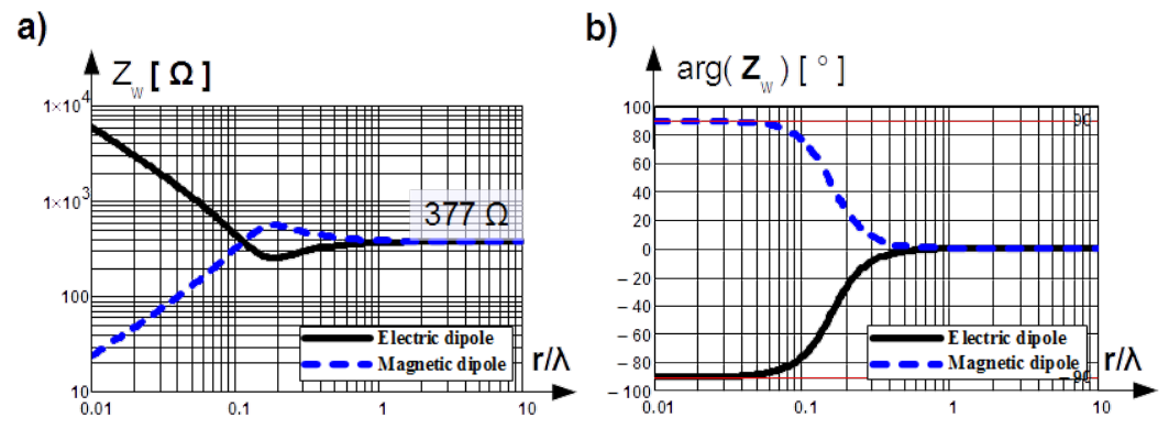
According to the rule of thumb it can be stated that the near field zone is within electrical distance [latex]r/\lambda<0.1[/latex]. By that distance the phase angle rises to [latex]-80^{\circ}[/latex] for electric dipole and decays to [latex]80^{\circ}[/latex] for magnetic dipole. Within that distance field is practically pure electric or magnetic. The same rule of thumb tells us to presume the far field zone in an electrical distance [latex]r/\lambda>1[/latex]. Memorize that the wave impedance in the far field zone regardless the direction approaches the intrinsic impedance Eq. (4.49)4, which for the vacuum and approximately for the air is [latex]Z_0 = 120 \pi[/latex] [latex]\Omega \approx 377[/latex] [latex]\Omega[/latex]. The wave impedance in the far field zone has resistive character and it represents real radiated power.
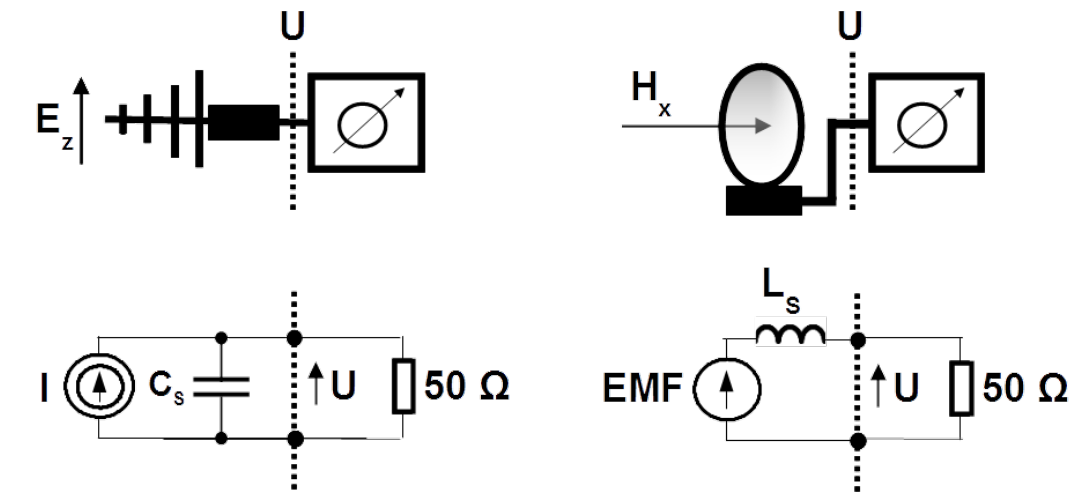
It is evident why the zone between [latex]0.1Field probes Probes are used for measurements of field strength in near and reactive zone. They should not distort incident field thats why they must be electrically small. This rationalizes their drawback namely moderate signal of response. Construction of the sensor in the field probe imitate electric or magnetic dipole with finite dimensions. Equivalent circuits are shown in Fig. 4.22. [latex]C_S[/latex] and [latex]L_S[/latex] are capacitance and inductance of the electric and magnetic sensor respectively. [latex]R_L[/latex] is resistance of the circuitry terminating the sensor.

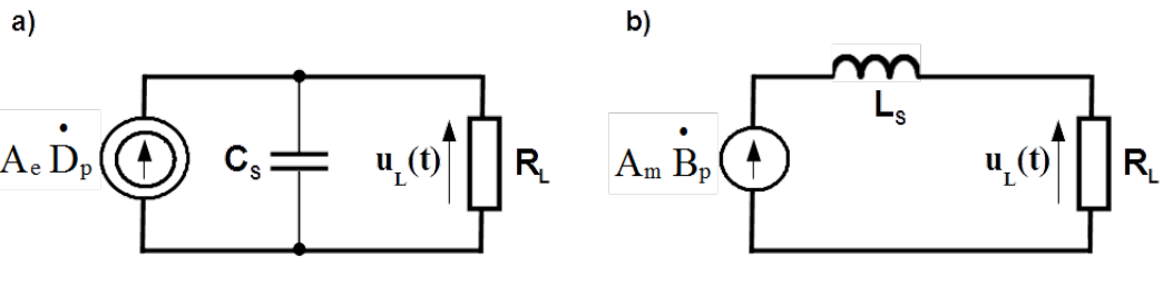
Output voltage [latex]u_L(t)[/latex] of the electric sensor is linked with the component of the density of the displacement current [latex]\overset{\bullet}{D}_p(t)[/latex] in the space point in which the sensor is placed and matched with the orientation of the probe, see Fig. 4.22a)
[latex]C_S \frac{du_L(t)}{dt} + \frac{u_L(t)}{R_L} = A_e \frac{dD_p(t)}{dt} = A_e \overset{\bullet}{D}_p(t) \label{u_e}\tag{4.68}[/latex]
[latex]A_e[/latex] is parameter of the probe transferring the component of the density of the displacement current [latex]\overset{\bullet}{D}_p(t)[/latex] to the current source in the equivalent circuit in Fig. 4.22a), expressed in area units. It is called equivalent surface.
In the frequency band of applications current driven through the capacitance [latex]C_S[/latex] is negligibly small and can be omitted. Then response [latex]u_L(t)[/latex] of the sensor is proportional to the component of the density of the displacement current [latex]\overset{\bullet}{D}_p(t)[/latex]. The sensor is a current source with magnetomotive force [latex]A_e \overset{\bullet}{D}_p(t)[/latex].
Current [latex]i(t)[/latex] in the mesh in Fig. 4.22b) is linked with the time derivative of the component of magnetic inductance [latex]\overset{\bullet}{B}_p(t)[/latex] in the space point in which the sensor is placed and matched with the orientation of the sensor
[latex]L_S \frac{di(t)}{dt} + R_L i(t) = A_m \frac{dB_p(t)}{dt} = A_m \overset{\bullet}{B}_p(t) \label{i_m}\tag{4.69}[/latex]
[latex]A_m[/latex] is parameter of the probe transferring the time derivative of the component of magnetic inductance [latex]\overset{\bullet}{B}_p(t)[/latex] to the voltage source in the equivalent circuit in Fig. 4.22b), expressed in area units. It is called equivalent surface.
In the frequency band of applications voltage across the inductance [latex]L_S[/latex] is negligibly small and can be omitted. Then response [latex]u_L(t)[/latex] of the sensor is proportional to the time derivative of the component of magnetic inductance [latex]\overset{\bullet}{B}_p(t)[/latex]. The sensor is a voltage source with electromotive force [latex]A_m \overset{\bullet}{B}_p(t)[/latex].
On the market are available directive and isotropic probes. The first sense only field component mached with the probe orientation, the second sense three orthogonal components of field in space.
There is variety of probes capable of capturing amplitude in overall frequency band of application. Directly by the sensor they have RF detector, most frequently diode one. Thereafter there is A/C converter and the signal is delivered either to the display integrated with the sensor in case of autonomous probe or is converted to light and transmitted via the fiber glass to the computer interface. Increasingly the fiber glass is used simultaneously for powering electronic by the sensor.
Probes are able to measure faithfully only CW i.e. single frequency fields. They are inapplicable for any modulated or transient fields.
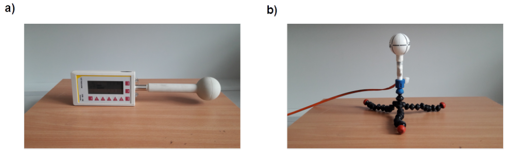
Example of autonomous isotropic probe for electric and magnetic field with the bandwidth from DC to 400 kHz is shown in Fig. 4.23a) and isotropic electric probe with optical transmission of signal and power applicable in the bandwidth from 10 kHz to 6 GHz in Fig. 4.23b).

There are other types of probes called in jargon D-dot and B-dot probes. They are applicable for measurements of pulsed fields. In such probes digital processing of the sensor response, which is proportional to the field derivative, see Eq. (4.68) and Eq. (4.69), is preceded with the time integration. They are exclusively directional probes.
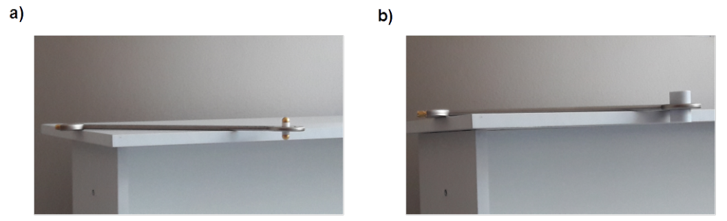
Example of free space directional D-dot probe with the bandwidth from from 100 kHz to 3.5 GHz is shown in Fig. 4.24a) and free space directional B-dot probe with the bandwidth from 100 kHz to 2 GHz in Fig. 4.24b).

Antennas
In technical terminology terms electric and magnetic antenna are used. The first concerns antennas with the wave impedance in the near field zone bigger than intrinsic impedance.
Antennas are used for selective measurements of stationary fields in the far field zone. It can be assumed that they do not distort incident field. Analogue voltage signal induced in the antenna is transmitted from the antenna terminal to the spectrum analyzer or other radio frequency selective measurement receiver which records frequency spectrum of the measured field.
Antennas for the measurement of electric fields are variations of electric dipoles. Dipole can be interpreted as unloaded symmetrical transmission line with straightened out conductors. The tips of dipole’s arms are nodes for current distribution and antinodes for voltage distribution. Current vanishes there and voltage varies from plus to minus amplitude due to open circuit condition.
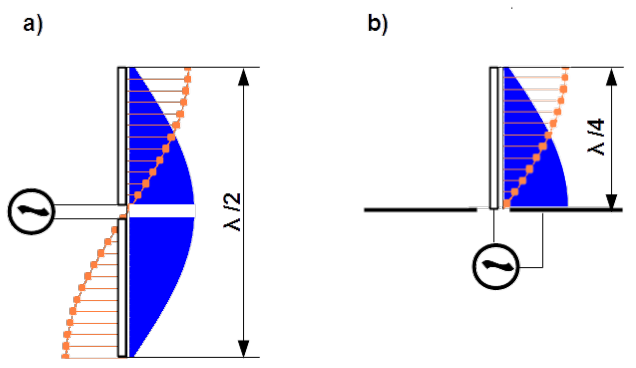
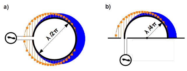
By [latex]\lambda/2[/latex] dipole as shown in Fig. 4.25a) the current distribution, the blue area is half of the approximately cosine function5 with amplitude in the midpoint between the arms i.e. by antenna terminal. Voltage distribution, the orange needles is half of the sine function with fixed zero value by antenna terminal and varying between plus and minus amplitudes at the tips.
In Fig. 4.25 b) a half dipole antenna is shown. Such miniature antennas are used as grounded probes of electric fields or much bigger as monopole (rod) receiving antennas.
Dipole radiate efficiently if its length is matched with approximately multiple of the half of the wavelength [latex]\lambda/2[/latex]. This efficiency is very sensitive on mismatching. In order to expand the frequency bandwidth rods in the ordinary dipole are replaced with conus (bi-conical antenna), triangle (bow-tie antenna) or more complex shapes by brad band antennas.
In Fig. 4.30 b) the bow-tie-log-periodic antenna is shown. Its frequency of operation extends from 30 MHz do 1500 MHz. The bow-tie section of the antenna, big triangles next to the feeding point covers frequency band from 30 MHz to about 300 MHz. It is connected parallelly with the Log-Periodic Dipole Antenna LPDA ahead. The LPDA is group of dipole antennas of varying sizes strung together. The dipole antennas diminish in size from the back to the front. The element at the back of the array which is the largest is tuned to frequency about 300 MHz and that at the front is a half wavelength at the highest frequency of operation i.e at 1500 MHz.
In the antenna boom between coaxial junction and bow-tie section a black box with the balun is mounted. Input of the dipole antenna is symmetric but the feeding point coaxial. The balun is a two port adapting symmetric to coaxial terminal. The name is a cluster of two words balanced-unbalanced.


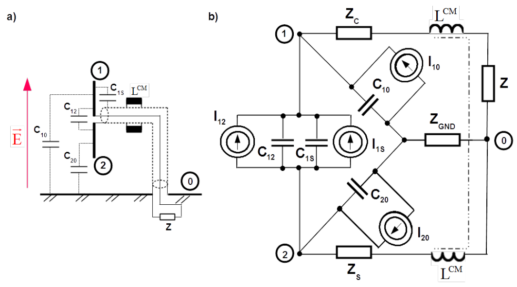
Desired signal of electric dipole stems from capacitance between the arms. It is [latex]C_{12}[/latex] in Fig.4.26 a). Additionally each arm has its own capacitance to the ground. They are [latex]C_{10}[/latex] and [latex]C_{20}[/latex]. There is still one more capacitance that must be taken into account. Namely between the arm connected to the core of the coaxial cable and the shield. It is arm 1 and capacitance [latex]C_{1S}[/latex] in Fig.4.26 a). Capacitance between the arm 2 and the cable shield is short circuited. [latex]Z[/latex] is the input impedance of the measurement receiver.
Equivalent circuit of the dipole is composed of parallel circuits of the current sources with their capacitances as it was explained for the free space electric sensor shown in Fig.4.22 a)6. In Fig.4.26 b) branch with [latex]Z_C[/latex] represents impedances of cable core, [latex]Z_S[/latex] cable shield and [latex]Z_{GND}[/latex] the ground reference. If capacitances [latex]C_{10}[/latex] and [latex]C_{20}[/latex] are different then they contribute to the differential current driven through the core, the measurement receiver and the shield. Moreover probable is also common mode current returning through the ground. Differential contribution of capacitances [latex]C_{10}[/latex] and [latex]C_{20}[/latex] cannot be eliminated. It overlays with desired signal [latex]I_{12}[/latex] causing distortion.
The current balun is simply ferrite mounted on the coaxial cable direct by junction with symmetrical antenna output. The common mode choke7 [latex]L^{CM}[/latex] shown in Fig. 4.26 suppresses common mode contribution of capacitances [latex]C_{10}[/latex] and [latex]C_{20}[/latex] but it does not eliminate it totally. Total elimination of differential and common mode distortion caused by capacitances [latex]C_{10}[/latex] and [latex]C_{20}[/latex] would happen if they were equal. Practically this condition is fulfilled by horizontal polarization of the antenna and very high above the ground reference, regardless polarization8.
There is still another parasitic capacitance [latex]C_{1S}[/latex] which contributes differentially to the desired signal, see Fig.4.26 b) and cannot be eliminated. The only way is to keep the capacitance small and place the common mode choke [latex]L^{CM}[/latex] as close as possible by antenna feeding.

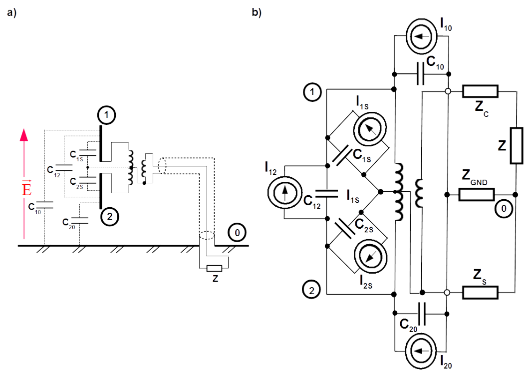
More sophisticated are voltage baluns, based on transformers. Example of one of them is shown in Fig. 4.27. Transformer separates galvanically symmetrical terminal of the antenna from coaxial cable connector. Additionally cable shield tapes the centre of the transformer winding on the symmetrical side. It has triple advantage:
- cancellation of the common mode distortion due to capacitances [latex]C_{10}[/latex] and [latex]C_{20}[/latex], thanks galvanic separation,
- both arms of the dipole are liberated from the potential of the cable shield, thanks galvanic separation,
- capacitances of both dipole arms to the cable shield [latex]C_{1S}[/latex] and [latex]C_{2S}[/latex] are equal one to another due to introducing the potential of the cable shield to the midpoint between the arms.
Contribution of the differential component in the distortion caused by unequal capacitances [latex]C_{10}[/latex] and [latex]C_{20}[/latex] is ruled in the same way same as by the current balun.
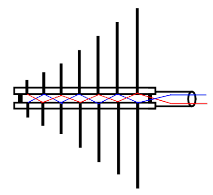
The balun in the antenna shown in Fig. 4.30 b) is necessary because of the bow-tie section. The LPDAs’ antennas are not finished with them. The adjacent dipoles in a LPDA antenna are connected to the symmetrical line routed inside the antenna (red and blue lines in Fig. 4.28) alternately. Consequently averaged capacitances of upper and lower arms to the cable shield and to the ground reference are equalized, minimizing distortion of the measured signal.

All precautions concerning symmetrization in the antenna can be spoiled with incorrect routing of the coaxial cable behind the antenna. In the document [@CISPR-16-1-4] two recommendations are formulated:
- by EMC testing of radiated emission the coaxial cable behind the antenna should be maintained horizontal, i.e. parallel to the ground plane, for a distance of approximately 1 m or more to the rear of the antenna before dropping to the ground plane,
- by verification of the anechoic chambers the coaxial cable behind the antenna should be oriented horizontally behind the antenna for a distance as close to 2 m as physically possible.
The LPDA antennas available on the market have booms with about 1 m length.


Antennas for the measurement of magnetic fields are variations of magnetic dipoles. Magnetic dipole can be interpreted as short circuited symmetrical transmission line with the circle shape. The junction point of upper and lower conductor is the node for voltage distribution and antinode for current distribution. Voltage vanishes there and current varies from plus to minus amplitude due to short circuit condition.
By [latex]\lambda/2[/latex] loop dipole9 as shown in Fig. 4.29 a) the current distribution, the blue area is half of the approximately cosine function with amplitude in the junction point of upper and lower conductor. Voltage distribution, the orange needles is half of the sine function with fixed zero value by the junction point of upper and lower conductor and varying between plus and minus amplitudes at the antenna feeding.
In Fig. 4.29 b) a half loop antenna is shown. Such loops with miniature size are used as grounded probes of magnetic fields.
Loop antennas are used in the frequency range up to 30 MHz. Their response is very week. The bigger radius the stronger response due to its dependence on magnetic flux streaming through the loop area. However lower location sensitivity by the measurements of inhomogeneous fields due to averaging of the flux with the loop area. By the loop antennas signal sensitivity and averaging effect must be always compromised. By active loop antenna with built in amplifier size of the loop can be reduced.
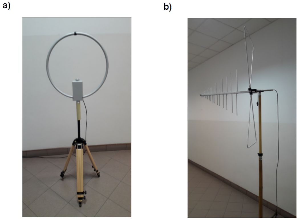
In Fig. 4.30 a) the loop antenna with frequency of operation from 9 kHz to 30 MHz is shown. In the box by the tripod the amplifier is placed. At the top of the antenna a black ring is visible. Loop antennas have metal tube around, which plays a role of electric shield. Thanks the shield picking up unwanted responses steaming from electric fields can be avoided. This shield however must be broken to prevent the metal tube from acting like a shorted turn. The plastic ring positions the free ends of the broken metal tube.
Antenna factor.
By measurements of radiated disturbances with antennas it is necessary to recalculate the signal at the input of the measurement receiver to the field strength to which the antenna is exposed. The antenna factor facilitates this conversion.
If receiving antenna is exposed to the field, electromotive force [latex]EMF[/latex] is induced in it. Antennas are not sensing the field module but the component matched with their orientation, [latex]E_z[/latex] or [latex]H_x[/latex] in Fig. 4.31. In other words induced [latex]EMF[/latex] depends on the projection of the field vector on the E-plane for electric and H-plane for magnetic antenna. [latex]Z_s[/latex] is the antenna impedance seen from its terminals.

By determining the antenna factor the antenna is oriented to the plane matching the field with known strength [latex]E_z[/latex] or [latex]H_x[/latex]. The instrument with [latex]50[/latex] [latex]\Omega[/latex] input resistance capable of HF voltage measurements, such as: power meter with insertion unit or power sensor, spectrum analyzer or measurement receiver, is connected to the terminals of the antenna. Ratio of field strength and voltage at the measuring instrument is the antenna factor.
[latex]\label{F_A} AF^{(E)}\left[\frac{1}{m} \right] = \frac{E_z}{U} \hspace{3cm} AF^{(H)}\left[\frac{1}{\Omega m} \right] = \frac{H_x}{U}\tag{4.70}[/latex]
In the [latex]dB[/latex] scale the units are [latex]dB[1/m][/latex] and [latex]dB[1/(\Omega m)][/latex] respectively. The antennas’ factors are determined for the far field zone in the air where wave and intrinsic impedances are identical [latex]E/H = Z_0 \approx 377[/latex] [latex]\Omega[/latex]. Alternatively manufacturers and calibration laboratories presents the factor for magnetic antennas as follows
[latex]AF^{(H)}\left[\frac{1}{ m} \right] = AF^{(H)} \left[dB\left(\frac{1}{\Omega m}\right) \right] + 51.5 [dB(\Omega)][/latex]
Surface power density.
Vector product of phasors of electric field strength and conjugate of magnetic field strength at arbitrary point in space builds the phasor of the Poynting’s vector
[latex]\overrightarrow{\bf{S}} = \overrightarrow{\bf{E}} \times \overrightarrow{\bf{H}}^* \label{Poynting_1}\tag{4.72}[/latex]
Surface integral of the phasor of the Poynting’s vector over any closed surface [latex]s[/latex], oriented outwards versus solid enclosing some antennas gives the phasor of total apparent power [latex]{\bf{P}}_{app}[/latex] on this surface [@Hammond_2]
[latex]{\bf{P}}_{app}=\oiint_s \left( \overrightarrow{\bf{E}} \times \overrightarrow{\bf{H}}^* \right) \cdot \overrightarrow{ds} \label{Power_app} \tag{4.73}[/latex]
crucial is that [latex]\overrightarrow{ds}[/latex] is the surface versor oriented outward versus the solid with antennas.
If phasors in Eq. (4.72) are scaled with RMS values then Poynting’s vector [latex]\overrightarrow{\bf{S}}[/latex] gives density per surface unit of apparent power at the point of interest10. Sense of the Pointing’s vector shows direction of power transportation in case of electric antennas and oposite direction in case of magnetic antennas. In the near and reactive field zone the imaginary part of the Poynting’s vector represents density of reactive power traveling back and forth between the antenna and the point of interest and real part represents density of real power radiated out of the antenna.

In the far field zone the imaginary part of the Poynting’s vector decays. It is actually attribute of the far field zone. There is no phase shift between fields’ strengths. Magnitude of the Poynting’s vector represents solely density of radiated power.
Each antenna, even geometrically complex is seen, from the observation point located at the wavefront, as the point radiator. Therefore three features of the dipoles’ fields in the far field zone can be extended to antennas with any shape. Two of them are listed below:
- the equiphase surface is the sphere,
- the field strength decreases in the far field zone reciprocally proportional to the distance.
For formulation of the third one, additional definition is necessary. It will be introduced later in this paragraph.
Let us imagine wavefront of an antenna with electric field strength polarized in the [latex]\varphi = const[/latex] plane and magnetic field strength polarized in the [latex]z = const[/latex] plane, green coloured in Fig. 4.32 a). The triple of the vectors can be oriented as shown there. The magnitude of the Poynting’s vector yields
[latex]S_r(r,\theta) = E_\theta(r,\theta) H_\varphi(r,\theta) = \frac{{E_\theta^2(r,\theta)}}{Z_0} = Z_0 {H_\varphi^2(r,\theta)} \label{Poynting_2}\tag{4.74}[/latex]
Let us imagine wavefront of an antenna with magnetic field strength polarized in the [latex]\varphi = const[/latex] plane and electric field strength polarized in the [latex]z = const[/latex] plane, green coloured in Fig. 4.32 b). The triple of the vectors can be oriented as shown there. The magnitude of the Poynting’s vector yields
[latex]S_r(r,\theta) = E_\varphi(r,\theta) H_\theta(r,\theta) = \frac{{E_\varphi^2(r,\theta)}}{Z_0} = Z_0 {H_\theta^2(r,\theta)} \label{Poynting_3}\tag{4.75}[/latex]
If the antenna in Fig. 4.32 a) is elementary electric dipole with strengths expressed with Eqs. (4.57) and (4.58) then
[latex]S^{(E)}_r(r,\theta) = \frac{p_z^2 \beta_0^2 Z_0 } {16 \pi^2 } \cdot \frac{\sin^2{\theta}}{r^2} \label{Poynting_4}\tag{4.76}[/latex]
Total power radiated by the electric dipole is equal to the surface integral of the Poynting vector Eq. (4.73) and can be calculated over equiphase sphere with arbitrary radius [latex]r[/latex].
[latex]P_{rad}^{(E)}=\unicode{x222F}_s S_r^{(E)} \overrightarrow{1}_r \cdot \overrightarrow{ds} = \unicode{x222F}_s S_r^{(E)} r^2 \sin{\theta} d\theta d\varphi =[/latex]
[latex]=\frac{p_z^2 \beta_0^2 Z_0 } {16 \pi^2 } {\int_{-\frac{\pi}{2}}^{\frac{\pi}{2}} \sin^3{\theta} d\theta} {\int_{0}^{2 \pi} d\varphi} = \nonumber[/latex]
[latex]= \frac{p_z^2 \beta_0^2 Z_0 } {6 \pi } \label{Power_rad} \tag{4.77}[/latex]
If the antenna in Fig. 4.32 b) is elementary magnetic dipole with strengths expressed with Eqs. (4.59) and (4.60) then
[latex]S^{(H)}_r(r,\theta) = -\frac{m_z^2 \omega^2 \mu_0^2 \beta_0^2 } {16 \pi^2 Z_0 } \cdot \frac{\sin^2{\theta}}{r^2} \label{Poynting_5}\tag{4.78}[/latex]
Total power radiated by the electric dipole is equal to the surface integral of the Poynting vector Eq. (4.73) and can be calculated over equiphase sphere with arbitrary radius [latex]r[/latex].
[latex]P_{rad}^{(H)}=\unicode{x222F}_s S_r^{(H)} \left( -\overrightarrow{1}_r \right) \cdot \overrightarrow{ds} = \unicode{x222F}_s S_r r^2 \sin{\theta} d\theta d\varphi = \nonumber[/latex]
[latex]=-\frac{m_z^2 \omega^2 \mu_0^2 \beta_0^2 } {16 \pi^2 Z_0 } {\int_{-\frac{\pi}{2}}^{\frac{\pi}{2}} \sin^3{\theta} d\theta} {\int_{0}^{2 \pi} d\varphi} = \nonumber[/latex]
[latex]= \frac{m_z^2 \omega^2 \mu_0^2 \beta_0^2 }{6 \pi Z_0 } \label{Power_rad_H} \tag{4.79}[/latex]
In Eqs. (4.76) and (4.78) is apparent that the surface power density in the far field zone of elementary radiators decreases reciprocally proportional to the distance [latex]r[/latex] in square. This is the third feature valid also for realised antennas with any shape and size.
Radiation pattern.
Ability of antennas to radiate electromagnetic energy in different directions is portrayed with radiation pattern. It is defined for electric, magnetic field strength as well as for radiated power in far field zone. The radiation pattern is a function built over equiphase surface. Its value represents vector magnitude or power density. For electric/magnetic antenna oriented along z-axis, as shown in Fig. 4.20 b)/Fig. 4.20 c) electric/magnetic field has only [latex]\theta[/latex] component dependent on all co-ordinates [latex]r[/latex], [latex]\theta[/latex] and [latex]\varphi[/latex]. Patterns normalized with maximal value are objective measures for comparison of antennas’ performance. They are independent on distance [latex]r[/latex]
[latex]F^{(E)}(\theta,\varphi) = \frac{E_\theta(r,\theta,\varphi)}{ E_{\theta_{max}}} \hspace{1.5cm} F^{(H)}(\theta,\varphi) = \frac{H_\theta(r,\theta,\varphi)}{ H_{\theta_{max}}} \label{F_EH}\tag{4.80}[/latex]
Obviously normalized pattern of power radiation yields, see Eq. ( 4.74)
[latex]F_P^{(E)}(\theta,\varphi)=\frac{S_r^{(E)}(r,\theta,\varphi)}{ S_{r_{max}}^{(E)}} = \left[ F^{(E)} (\theta,\varphi) \right]^2[/latex]
[latex]\nonumber[/latex]
[latex]F_P^{(H)}(\theta,\varphi)= \frac{S_r^{(H)}(r,\theta,\varphi)}{ S_{r_{max}}^{(H)}} = \left[ F^{(H)} (\theta,\varphi) \right]^2 \label{F_S} \tag{4.82}[/latex]
Radiation pattern of field strength of the electric and magnetic dipole according to Eq. (4.57) and Eq. ( 4.60) are identical
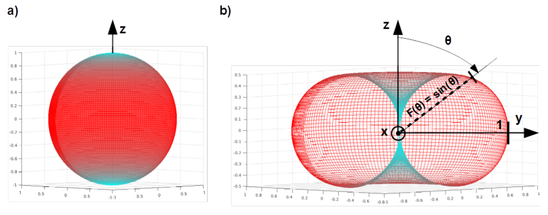
[latex]F^{(E)}(\theta) = F^{(H)}(\theta) = F(\theta) = \sin{(\theta)} \label{F_pm}\tag{4.84}[/latex]

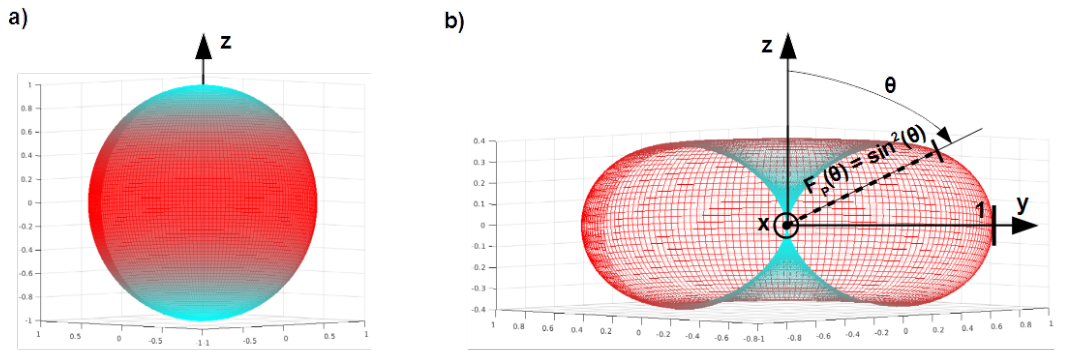
and of surface power density
[latex]F^{(E)}_P(\theta) = F^{(H)}_P(\theta) = F_P(\theta) = \sin^2{(\theta)} \label{F_pma}\tag{4.84}[/latex]

Radiation pattern of field strength of the electric and magnetic dipole in the spherical system of coordinates [latex]r, \theta, \varphi[/latex] is function of one variable [latex]\theta[/latex]. In the system of Cartesian coordinates [latex]x, y, z[/latex] it is function of all variables and can be depicted as a map of colours on the surface of the sphere with radius [latex]r=1[/latex], as shown in Fig. 4.33 a). From the engineer point of view such picture is useless.
Antennas’ engineers are accustomed with mapping the one variable pattern [latex]F(\theta)[/latex] into the two variables pattern [latex]F(r,\theta)[/latex] in which [latex]r = \sin{(\theta)}[/latex]. Such surface is the torus (doughnut) without hole in centre with circular cross-section in the plane [latex]\theta = 90^{\circ}[/latex] with radius [latex]r = 1[/latex] and two excentrically placed touching circles with radii equal [latex]0.5[/latex]. Distance between the origin of the Cartesian system of coordinates and the point at the pattern’s surface is equal to the value of the field strength by that elevation [latex]\theta[/latex], see Fig. 4.33 b). From such portrait radiation ability can be directly determined quantitatively.
The same concerns the pattern of the surface power density which is identical for both dipoles. In the spherical system of coordinates [latex]r, \theta, \varphi[/latex] it is function of one variable [latex]\theta[/latex]. In the system of Cartesian coordinates [latex]x, y, z[/latex] it is function of all variables and can be depicted as a map of colours on the surface of the sphere with radius [latex]r=1[/latex], as shown in Fig. 4.34 a). Usually it is mapped into the two variables pattern [latex]F(r,\theta)[/latex] in which [latex]r = \sin^2{(\theta)}[/latex]. Such surface is the vertically squeezed torus (doughnut) without hole in centre with circular cross-section in the plane [latex]\theta = 90^{\circ}[/latex] with radius [latex]r = 1[/latex] and two excentrically placed touching, deformed circles. Distance between the origin of the Cartesian system of coordinates and the point at the pattern’s surface is equal to the value of the surface power density by that elevation [latex]\theta[/latex], see Fig. 4.34 b).
Solid representing the two variables radiation pattern [latex]F(r,\theta)[/latex] is called the lobe. The electric as well as magnetic dipole has only one lobe which is the torus. The realized antennas have so called main lobe roundabout the desired radiation direction and usually more than one side lobe which is undesired, side effect causing waste of radiated power.
Dipoles and antennas presented up to now are oriented along z-axis of the global system of coordinates i.e. vertically. For presentation of radiation pattern at the plane, as it is usually the case in the antennas’data sheets, it is more convenient to use system of coordinates tied to the antenna. Then the cross-section including only electric field component or magnetic field component is called E-plane or H-plane respectively. For the dipole in Figs. 4.33 b) and 4.34 b), the presented cross-section is the E-plane if it is electric dipole and H-plane if it is magnetic dipole. The cross-section [latex]\theta = 90^{\circ}[/latex] would be H-plane for electric dipole and E-plane for magnetic dipole.
Directive gain and directivity.
Compared is antenna under interest with isotropic antenna radiating the same power. Directive gain [latex]D(r,\theta)[/latex] is ratio of the surface radiated power of the first and the second. Directivity is maximal value of the directive gain. Both parameters gives the measure of squeezing the power beam referred to the omnidirectional radiation.
Let us derive these parameters for the electric and magnetic dipole as shown in Fig. 4.20 b) and c). Division of total radiated power of the electric dipole Eq. (4.77) and magnetic dipole Eq. (4.79) by the solid angle of the sphere [latex]4\pi r^2[/latex] gives surface power density of the isotropic antenna
[latex]S_i(r) = \frac{p_z^2 \beta_0^2 Z_0 } {24 \pi^2 r^2 } \hspace{2cm} S_i(r) = \frac{m_z^2 \omega^2 \mu_0^2 \beta_0^2 } {24 \pi^2 Z_0 r^2 } \label{Poynting_i}\tag{4.85}[/latex]
According to the definition, the directive gain is fraction of surface power density of the dipole and density of isotropic radiator Eq. (4.85). The numerator in this fraction is Eq. (4.76) by the electric dipole and Eq. (4.78) by the magnetic dipole
[latex]D(\theta) = \frac{3 } {2 } \sin^2{\theta} \label{Directivity_1}\tag{4.86}[/latex]
and directivity
[latex]D_{max} = D(90^{\circ}) = \frac{3 } {2 } \label{Directivity_2}\tag{4.87}[/latex]
In the [latex]dB[/latex] scale [latex]D_{max} \approx 1.8[/latex] [latex]dB_i[/latex]11. In the direction of the maximal radiation, the dipole radiates 50% or [latex]1.8[/latex] [latex]dB_i[/latex] more power then isotropic radiator with the same totally radiated power.
(Energetic) gain,
usually named simply gain is the directivity diminished by energetic efficiency of the antenna [latex]\eta[/latex] defined as ratio of total power radiated by the antenna [latex]P_{rad}[/latex] and power at the antenna feeding port [latex]P_{in}[/latex]
[latex]G_i = \eta D_{max} = \frac{P_{rad}}{P_{in}} D_{max} \label{Gain}\tag{4.88}[/latex]
By interpretation of power at the antenna feeding port [latex]P_{in}[/latex] ambiguity can creep in. If net power12 is introduced as the input power [latex]P_{in} = P_{fwr} - P_{rev}[/latex] then the gain is preceded with the adjective absolute. If forward power sent from the signal source is introduced as the input power [latex]P_{in} = P_{fwr}[/latex] then the gain is preceded with the adjective realised. By absolute gain, unlike by realised gain mismatching at the feeding point is taken into account. Be prudent by evaluation of catalogue data of an antenna in respect of its gain.
More practical meaning has the gain [latex]G_d[/latex] referred to the half wave dipole. Since the gain of the half wave dipole referred to the isotropic antenna is [latex]1.64[/latex] in the linear scale and [latex]2.15[/latex] [latex]dB_i[/latex], see [@Clayton]
[latex]G_d=\frac{1}{1.64} G_i[/latex]
[latex]& \nonumber[/latex]
[latex]G_{{dB}_d}=G_{{dB}_i} - 2.15dB_i \label{G_d} \tag{4.90}[/latex]
Equivalent isotropically radiated power EIRP
is the input power at the terminal of the isotropic radiator necessary for radiation with the surface power density equal to the maximum of the magnitude of the surface power density [latex]S(r)[/latex] of the considered antenna in the far field zone. It is product of this value and solid angle of the sphere
[latex]EIRP = 4 \pi r^2 |S(r)|_{max} \label{EIRP}\tag{4.91}[/latex]
The EIRP does not depend on the distance [latex]r[/latex]. Indeed the EIRP is explicitly proportional to the distance [latex]r[/latex] in square but reciprocal proportionality to distance [latex]r[/latex] in square is implied in the [latex]|S(r)|_{max}[/latex] due to attribute of the far field zone.
For the electric dipole calculation is based on Eq. (4.76) and for magnetic dipole on Eq. (4.78) with setting [latex]\theta = 90^{\circ}[/latex]
[latex]EIRP^{(E)} = \frac{p_z^2 \beta_0^2 Z_0 }{4 \pi } \hspace {1.5cm} EIRP^{(H)} = \frac{m_z^2 \omega^2 \mu_0^2 \beta_0^2 }{4 \pi Z_0 } \label{EIRP_EH}\tag{4.92}[/latex]
Let us derive the measurement procedure of the EIRP for an electric antenna. The set up is established in the full anechoic chamber in which walls, ceiling and floor are lined with the absorbers marked with pyramids in Fig. 4.35, simulating reflection free space. The investigated antenna [latex]T_x[/latex] and receiving antenna [latex]R_x[/latex] are placed at the same height above the floor in order to match their elevations with [latex]\theta = 90^{\circ}[/latex]. The investigated antenna must be rotated about the vertical axis to the azimuth maximizing signal [latex]U_R[/latex] in the measurement receiver and fixed in this position.

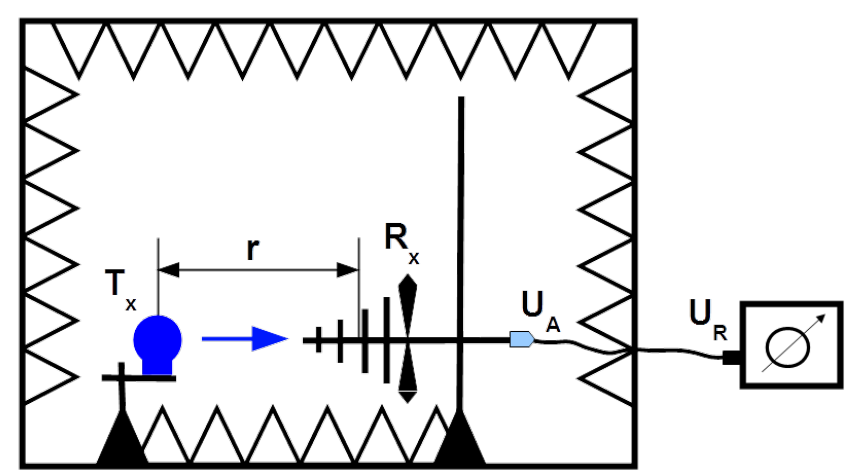
Applied must be Eq. (4.74) for surface power density in the direction of maximal radiation i.e. by elevation [latex]\theta = 90^{\circ}[/latex] and Eq. (4.31) for antenna factor of an electric antenna
[latex]S_r(r,90^{\circ}) = \frac{E_{\theta}^2(r,90^{\circ})}{Z_0} = \frac{\left( AF^{(E)} \right)^2}{Z_0} U_A^2(r) \label{EIRP_2}\tag{4.93}[/latex]
For EIRP this formula must be multiplied by the solid angle of the sphere
[latex]EIRP = \frac{4 \pi r^2}{Z_0} \left( AF^{(E)} \right)^2 U_A^2(r) \label{EIRP_3}\tag{4.94}[/latex]
Requested unit for the EIRP is [latex]mW[/latex] and for voltage at the antenna terminal [latex]\mu V[/latex]. Suitable formula yields
[latex]EIRP \left[ mW\right] = \frac{4 \pi r^2 \left[m^2 \right]}{377 [\Omega]} \left( AF^{(E)} \right)^2 \left[ \frac{1}{m^2}\right] U_A^2(r) \left[(\mu V)^2 \right] 10^{-9} \label{EIRP_4}\tag{4.95}[/latex]
Both sides of equation are logarithmised and multiplied by 10
[latex]EIRP_{_{dB(mW)}}(r)= 10\log{ \left( \frac{4 \pi r^2 \left[ m^2 \right] }{377 [\Omega]} \right)} - 90_{_{dB}}+ 20\log{ \left\{ AF^{(E)}\left[ \frac{1}{m} \right] \right\}} + \nonumber[/latex]
[latex]\nonumber[/latex]
[latex]& +A_{C_{dB}} + 20\log{ \left\{ U_R(r) \left[ \mu V \right] \right\} } \label{EIRP_5} \tag{4.96}[/latex]
Voltage at the feeding terminal of the receiving antenna [latex]U_{A_{dB(\mu V)}}[/latex] is greater than voltage measured by the receiver [latex]U_{R_{dB(\mu V)}}[/latex] about attenuation [latex]A_{C_{dB}}[/latex] of the measurement path (cables, feed through) [latex]U_{A_{dB(\mu V)}} (r) = A_{C_{dB}} + U_{R_{dB(\mu V)}} (r)[/latex]
[latex]EIRP_{_{dB(mW)}}(r)= \left[10\log{ \left( \frac{4 \pi r^2 }{377} \right)} - 90_{_{dB}} \right]+ AF_{_{dB(1/m)}}^{(E)} + \nonumber[/latex]
[latex]\nonumber[/latex]
[latex]& +A_{C_{dB}} + U_{R_{dB(\mu V)}} (r) \label{EIRP_6} \tag{4.98}[/latex]
The EIRP is independent on distance [latex]r[/latex]. Indeed there is radius in square in the numerator in Eqs. from (4.94) to (4.98) but measurement is done in the far field zone in which surface power density decreases reciprocally proportional to the distance in square. Consequently the same concerns the voltage at the antenna terminal. By increasing distance e.g. three times the term in square bracket in Eq. (4.98) increases about 9.5 dB but in the same time the voltage at the antenna terminal [latex]U_{A_{dB(\mu V)}}[/latex] and consequently at the receiver input [latex]U_{R_{dB(\mu V)}}[/latex] decreases about the same amount.
Typical distance for performing the measurements of the EIRP is ([latex]r= 3[/latex] [latex]m[/latex]). By doing so correction factor in the square brackets is [latex]-95.2_{{dB}}[/latex].
Radiation resistance
Total radiated power is represented in the equivalent circuit of the antenna with radiation resistance [latex]R_{rad}[/latex] through which current [latex]I[/latex] from the source feeding antenna is driven [latex]R_{rad}I^2[/latex].
Let us calculate this resistance for the electric dipole. Total radiated power is ruled with Eq. (4.77). Replacing the magnitude of dipole moment with the product of current magnitude [latex]I[/latex] and infinitesimal segment [latex]l[/latex] Eq. (4.41), moreover with implementing the wavelength [latex]\lambda_0[/latex] instead of the phase constant [latex]\beta_0[/latex], according to Eq. (4.50) yields
[latex]R_{rad}^{(E)} = \frac{2 \pi Z_0}{ 3} \left(\frac{l}{\lambda_0} \right)^2 \label{R_rad}\tag{4.99}[/latex]
In vacuum and approximately in air this resistance is [latex]R_{rad}^{(E)} \approx 789.57 \left( \frac{l}{\lambda_0} \right)^2 [\Omega][/latex] if the dipole length [latex]l[/latex] and the wavelength [latex]\lambda_0[/latex] have the same units.
In feasible short dipole relation [latex]l/\lambda_0[/latex] and consequently radiation resistance is very small. Therefore radiation ability is very weak13.
For example, for a length ([latex]l = 1[/latex] cm) and a frequency of 300 MHz ([latex]\lambda_0 = 1[/latex] m), the radiation resistance is [latex]R_{rad}^{(E)} \approx 79 [m\Omega][/latex] In order to radiate 1 W of power, required is current of 3.6 A!
If the frequency is changed to 3 MHz ([latex]\lambda_0 = 100[/latex] m), the radiation resistance is [latex]R_{rad}^{(E)} \approx 7.9 \left[ \mu \Omega \right][/latex] and the current required to radiate 1 W is 356 A!
Moreover resistance [latex]R_{rad}[/latex] is serially circuited with the element representing antenna outlet to the lossless space. Depending on electrical length of the dipole [latex]l/\lambda_0[/latex] it can be capacitance, shortcircuit or inductance but for a short dipole it is huge capacitance limiting current driven through radiation resistance. It is the second factor contributing to very small radiation efficiency of the Hertzian as well as short dipole.
Let us proceed now to the radiation resistance of magnetic dipole. Total radiated power is ruled with Eq. (4.79). Replacing the magnitude of dipole moment with the product of current magnitude [latex]I[/latex] and infinitesimal loop area [latex]\pi a^2[/latex] Eq. (4.42), moreover with implementing the wavelength [latex]\lambda_0[/latex] instead of the phase constant [latex]\beta_0[/latex], according to Eq. (4.50) and relation [latex]\omega = 2 \pi v/\lambda_0[/latex] between angular frequency, wave velocity [latex]v[/latex] and wavelength yields [latex]\omega \beta_0 = \frac{4 \pi^2}{\lambda_0^2} v[/latex]
Finally
[latex]R_{rad}^{(H)} = \frac{8 \pi^3 \mu_0^2 v^2}{ 3 Z_0} \left( \frac{\pi a^2}{\lambda_0^2} \right)^2 \label{R_rad_H}\tag{4.104}[/latex]
Value of the wave speed in vacuum is given in Eq.([v_0]) therefore this resistance in air is approximately [latex]R_{rad}^{(H)} \approx 31'170.91 \left( \frac{\pi a^2}{\lambda_0^2} \right)^2 [\Omega][/latex]
if radius [latex]a[/latex] and wavelength [latex]\lambda_0[/latex] have the same units.
Consider a loop of radius ([latex]a= 1[/latex] cm). At 300 MHz the wavelength ([latex]\lambda_0 = 1[/latex] m) and the radiation resistance is [latex]R_{rad}^{(H)} \approx 3.08 \mu \Omega[/latex] In order to radiate 1 W, the loop requires a current of 18 A!
At 3 MHz the wavelength ([latex]\lambda_0 = 100[/latex] m) and the radiation resistance is [latex]R_{rad}^{(H)} \approx 30.8 p \Omega[/latex] and current required to radiate 1 W is 180 kA!
Both elementary dipoles radiate very weakly but their comparison shows that magnetic dipole is overwhelmingly worse radiator than electric. In practice they are scarcely met as unintentional antennas.
Half power beamWidth HPBW
called also 3 dB beamwidth is an angle span, either in azimuth or in elevation between two directions encompassing set of directions with the surface power density decaying not more then to the half of the maximum. In other words not reduced about more then 3 dB.

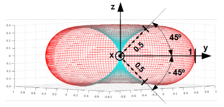
The electrical dipole is omnidirectional in respect to azimuth [latex]\varphi[/latex], therefore determining the HPBW on the plane [latex]\theta = 0^{\circ}[/latex] is groundless. For the elevation14 the upper bound is [latex]\theta = 45^{\circ}[/latex] and lower bound [latex]\theta = 135^{\circ}[/latex] therefore [latex]HPBW = 90^{\circ}[/latex], see Fig. (4.36).
HPBW expresses spreading of the power beam. The narrower HPBW, the better concentration of radiated power roundabout desired direction.
Unintentional antennas
It is mentioned frequently, that any cable can be either transmitting or receiving antenna.
By the measurement of radiated emission of the table top equipments in the Semi Anechoic Chamber SAC, the EUT must be placed on the table with 80 cm height. The mains cord should be stretched towards the table edge, dropped down towards the floor and plugged in the supply socket under the metal floor. Typical arrangement of the mains cord is shown in Fig. 4.37 a). Such cable is a monopole antenna while the EUT case is its ground reference. If the common mode current is driven in the cord and the cord length is matched with the wavelength, then the cable radiate and it is very often the case.

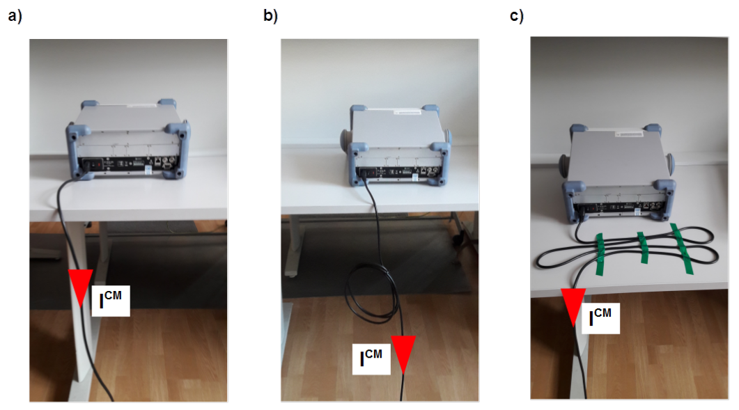
In Fig. 4.37 b) excess cable is arranged as it should not be. It is wound in few turns building the loop antenna. If the common mode current is driven in the cord and the loop diameter is matched with the wavelength, then it can radiate. Excess cable should be folded to and forth in order to form a low inductive bundle as shown in Fig. 4.37 c).
Let’s consider the metal case with the primary plane wave inside, propagating towards the wall with vector’s orientation of: electric field [latex]\overrightarrow{E}_p[/latex], magnetic field [latex]\overrightarrow{H}_p[/latex] and Poynting vector [latex]\overrightarrow{S}_p[/latex] as shown in the side projection in Fig. 4.38 b). By continuous metal wall of the case, surface current would be induced on the internal surface of the wall. The slot enables the current to leak outside. It flows on the external surface of the wall, in surrounding of the slot as shown with reddish region in Fig. 4.38 a). Black arrows on the edges of the slot shows direction of the driven current. It is accompanied with electric field in the vicinity of the slot oriented as vector [latex]\overrightarrow{E}[/latex] in Fig. 4.38 b). Imagine that the edges of the slot build two dipoles shortcircuited at the top of the arms. Such entity can hardly radiate due to cancellation in the far field zone. But as shown with the reddish region in Fig. 4.38 a) current is driven also on the external surface around the edges.

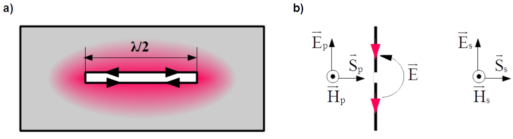
Therefore the secondary wave oriented as shown with the vectors of: electric field [latex]\overrightarrow{E}_s[/latex], magnetic field [latex]\overrightarrow{H}_s[/latex] and Poynting vector [latex]\overrightarrow{S}_s[/latex] in the side projection in Fig. 4.38 b) propagates from the case, particularly by matching the slot length. Example is [latex]\lambda/2[/latex] matching shown in Fig. 4.38 a). Memorize that orientation of the propagated field is dual to the electric dipole. Horizontally oriented slot propagates vertically oriented electric field.

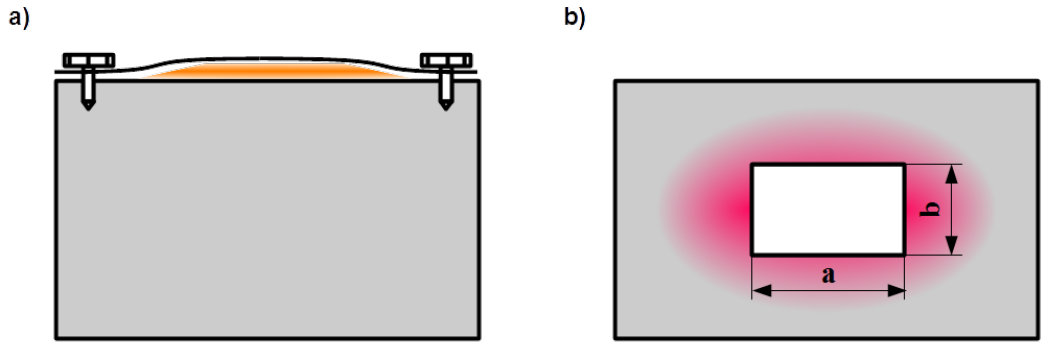
By point wise techniques of joining parts of the metal cases with screws, nuts or spot welding, gaps between places tied together, marked with yellowish area in Fig. 4.39 a) are formed. Things like incertitude of joined edges and deformations caused by excessed contact pressing force are contribution factors of it. In order to reduce effect of secondary radiation from such gaps distances between fixed spots must ensure length mismatching or/and EMC gaskets obstructing electromagnetically the gaps must be applied.
Windows and openings in cases are indispensable. They serves for mounting displays, cameras, switches, buttons, as sight hole or for ventilation and manipulation of the arrangement. Due to the same rules as by the gaps in the metal case the surface currents flow on the external surface of the wall as shown with the reddish area in Fig. 4.39 b). The window can build aperture antenna enabling the secondary wave to radiate out of the case.
There is alway maximal frequency called cut off, up to which the window is not capable to radiate. It is associated with the biggest wavelength which can be radiated. Above the cut off frequency the wavelength for the rectangular window with sides [latex]ab[/latex] and the circular window with the radius [latex]r[/latex] are approximately ruled with following inequalities
[latex]\begin{array} {cc} \lambda_{\framebox[0.15in]{}} < 2 \sqrt{\pi a b} & \hspace{2cm} \lambda_{\bigcirc} < 2 \pi^{\frac{3}{2}} r \approx 11.14 r \end{array} \label{cut_off_1}\tag{4.108}[/latex] Inequality for the circular window is convergent with matching of the circumference of the magnetic dipole to the [latex]\lambda/2[/latex] wavelength [latex]\lambda \approx 12.57 r[/latex] as illustrated in Fig. 4.29. It is also in line with condition of not being electrically small i.e. bigger than [latex]0.1 \lambda[/latex], see subsection [El_size].
Guided waves
So far in the chapter 4.4 we have been discussing conveying energy, signals and disturbances with radiation. By this art of transportation both field vectors [latex]\overrightarrow{E}[/latex] as well as [latex]\overrightarrow{H}[/latex] are perpendicular to the direction of propagation. This type of waves is called TEM (transverse electric magnetic) mode. The same TEM mode is present in transmission lines elaborated by galvanic coupling in chapter 4.2 as well as by electric and magnetic coupling in chapter 4.3. Transportation passed along the line and fields are perpendicular to it15. Therefore TEM mode is often referred to as the transmission line mode.

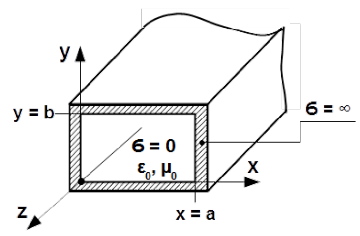
Let us consider tubular structure with rectangular cross-section, built of perfectly conducting material [latex]\sigma = \infty[/latex] filled with lossless dielectric [latex]\sigma = 0[/latex] with dielectric permittivity [latex]\epsilon_0[/latex] and magnetic permeability [latex]\mu_0[/latex] as shown in Fig. 4.40. Since [latex]\overrightarrow{E}[/latex] must be always perpendicular and [latex]\overrightarrow{H}[/latex] always tangential to the boundary, it is not possible to excite TEM in such structure.
Let us assume that in such structure propagates wave with three component of phasor’s electric field: two cross-sectional [latex]{\bf{E}}_x(x,y,z)[/latex], [latex]{\bf{E}}_y(x,y,z)[/latex] and longitudinal [latex]{\bf{E}}_z(x,y,z)[/latex]. The last is governed with the partial differential equation called the wave equation
[latex]\nabla^2 {\bf{E}}_z + \omega^2 \mu_0 \epsilon_0 {\bf{E}}_z = 0 \label{Ez_1}\tag{4.109}[/latex]
This equation can be solved by the method of separation of variables [latex]{\bf{E}}_z(x,y,z) = {\bf{X}}(x) {\bf{Y}}(y) {\bf{Z}}(z)[/latex]
[latex]\frac{{\bf{X}}^{''}}{{\bf{X}}} + \frac{{\bf{Y}}^{''}}{{\bf{Y}}} + \frac{{\bf{Z}}^{''}}{{\bf{Z}}} + \beta_0^2 = 0 \label{Ez_2}\tag{4.110}[/latex]
where [latex]\beta_0[/latex] is phase constant as defined in Eq. (4.50).
Eq. (4.110) can be split into three independent ordinary differential equations
[latex]\label{X} {\bf{X}}^{''} - {\bf\gamma}_x^2 {\bf{X}} = 0 \tag{4.111}[/latex]
[latex]\label{Y} {\bf{Y}}^{''} - {\bf\gamma}_y^2 {\bf{Y}} = 0 \tag{4.112}[/latex]
[latex]\label{Z} {\bf{Z}}^{''} - {\bf\gamma}_z^2 {\bf{Z}} = 0 \tag{4.113}[/latex]
along with dispersion equation
[latex]{\bf\gamma}_x^2 + {\bf\gamma}_y^2 + {\bf\gamma}_z^2 + \beta_0^2 = 0 \label{Ez_4}\tag{4.114}[/latex]
where [latex]{\bf\gamma}_x[/latex], [latex]{\bf\gamma}_y[/latex] and [latex]{\bf\gamma}_z[/latex] are separations’ constants.
Solution of Eq. (4.111) is following linear combination of waves [latex]{\bf{X}}(x) = A e^{{\bf\gamma}_x x} + B e^{-{\bf\gamma}_x x}[/latex] traveling forth and back along x axis. [latex]{\bf\gamma}_x x = \alpha_x + j\beta_x[/latex] can be a complex quantity. As [latex]E_z[/latex] is tangential to the walls of the waveguide but tangential component of electric field must be zero on perfectly conducting metal wall, [latex]{\bf{X}}(x)[/latex] must disappear by [latex]x =0[/latex] and [latex]x= a[/latex]. This is possible only if [latex]\alpha_x = 0[/latex]. Consequently magnitude [latex]X(x)[/latex] is a standing wave with the nodes on walls
[latex]X_m(x) = (A_m - B_m) \sin{(\beta_{x,m}}x) = X_{0,m} \sin{(\beta_{x,m} x)}[/latex]
[latex]\beta_{x,m} = m \frac{\pi}{a} \label{beta_x}\tag{4.117}[/latex]
where [latex]m[/latex] is integer number.
Identical procedure applied to Eq. (4.112) yields [latex]Y_n(y) = Y_{0,n} \sin{(\beta_{y,n} y)}[/latex] along with
[latex]\beta_{y,n} = n \frac{\pi}{b} \label{beta_y}\tag{4.119}[/latex]
where [latex]n[/latex] is integer number.
Solution of Eq. (4.113) is following linear combination of waves [latex]{\bf{Z}}(z) = C e^{{j\gamma}_z z} + D e^{{-j\gamma}_z z}[/latex] traveling back [latex]C e^{{j\gamma}_z z }[/latex] and forth [latex]D e^{{-j\gamma}_z z}[/latex] along the z-axis. The waveguide is infinite in respect to z-axis. Therefore physical meaning has only one wave.
The source of field is placed somewhere in the waveguide. From that location on, two waves propagate: one forwards another backwards in respect to z-axis. Assuming that source of field is placed by [latex]z<0[/latex] so that by [latex]z=0[/latex] regular propagation takes place, then by [latex]z \ge 0[/latex] propagates only [latex]{\bf{Z}}_{mn}(z) = D_{mn} e^{-{\bf\gamma}_{z,mn} z} \label{Z_2}\tag{4.121}[/latex] where [latex]{\bf\gamma}_{z,mn}^2 = - \beta_0^2 - \left( {\bf\gamma}_{x,mn}^2 + {\bf\gamma}_{y,mn}^2 \right) = \beta_{x,mn}^2 + \beta_{y,mn}^2 - \beta_0^2 \label{gamma_z}\tag{4.125}[/latex] [latex]{\bf\gamma}_{z,mn}[/latex] can be real, imaginary or can have zero value by the break point which corresponds to the cut-off frequency [latex]f_{c,mn}[/latex] [latex]f_{c,mn} = \frac{v_0}{2} \sqrt{\left( \frac{m}{a} \right)^2 + \left( \frac{n}{b}\right)^2} \label{gamma_zz}\tag{4.123}[/latex] where [latex]v_0[/latex] is wave velocity in vacuum and indexes [latex]mn[/latex] corresponds to Eqs. (4.117) and (4.119). Finally separation constant [latex]{\bf{\gamma}}_{z,mn}[/latex] which is identical with propagation constant in z direction is [latex]{\bf{\gamma}}_{z,mn} = \left\{ \begin{array} {ll} \frac{\omega}{v_0}\sqrt{ \left( \frac{f_{c,mn}}{f} \right)^2 - 1} & \text{for}~~f < f_{c,mn}\\ \\ j\frac{\omega}{v_0} \sqrt{ 1 - \left( \frac{f_{c,mn}}{f} \right)^2 } & \text{for}~~f > f_{c,mn} \end{array} \right. \label{gamma_z2}\tag{4.124}[/latex]
and z component of the phasor of electric field
[latex]{\bf{E}}_{z,mn}(x,y,z) = E_{z,mn}(0) \sin{\left(\frac{ m\pi }{a}x \right)} \sin{\left(\frac{n \pi }{b}y \right)} e^{-\gamma_{z,mn} z} \label{gamma_z}\tag{4.125}[/latex]
[latex]E_{z,mn}(0)[/latex] is product of [latex]X_{m}0[/latex], [latex]Y_{n}0[/latex] and [latex]D_{mn}[/latex]. For unique solution the value [latex]E_{z,mn}(0)[/latex] must be known.
Derivation of remaining field components can be found for instance in [@Hammond_2].
Eq. (4.125) can be rearranged with introduction of phase constant by propagation in free space with cut-off frequency [latex]\beta_0(f_{c,mn})[/latex]
[latex]{\bf{\gamma}}_{z,mn} = \left\{ \begin{array} {ll} \beta_0({f_{c,mn}}) \sqrt{ 1 - \left( \frac{f}{f_{c,mn}} \right)^2 } & \text{for}~~\frac{f}{f_{c,mn}} < 1\\ \\ j\beta_0({f_{c,mn}}) \sqrt{ \left( \frac{f}{f_{c,mn}} \right)^2 - 1} & \text{for}~~\frac{f}{f_{c,mn}} > 1 \end{array} \right. \label{gamma_z3}\tag{4.126}[/latex]
Dependence of the module of the propagation constant [latex]|\gamma_z|[/latex] versus frequency related to the cut-off frequency [latex]f/f_{c,mn}[/latex] is shown in Fig.4.41.

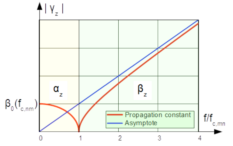
Below the cut-off frequency (yellowish region) the propagation constant is real [latex]\gamma_z = \alpha_z[/latex]. The wave is attenuated. Above the cut-off frequency (greenish region) the propagation constant is imaginary [latex]\gamma_z = j\beta_z[/latex]. The wave is able to propagate. The propagation constant in this region approaches asymptote [latex]\beta_{z,mn} = \beta_0 \left(f_{c,mn} \right) \frac{f}{f_{c,mn}}[/latex]
It is blue strait line in Fig.4.41.
The type of fields discussed up to now are so called E-mode named equivalently TM-mode. Notice that the lowest mode of this type of fields can be [latex]E_{11}[/latex] ([latex]TM_{11}[/latex]) due to constraint on tangential component of E field on the walls.
Similarly [latex]H_z[/latex] component for the H mode (TE) mode can be derived
[latex]{\bf{H}}_{z,mn}(x,y,z) = H_{z,mn}(0) \cos{\left(\frac{ m\pi }{a}x \right)} \cos{\left(\frac{n \pi }{b}y \right)} e^{-\gamma_{z,mn} z} \label{gamma_z4}\tag{4.128}[/latex]
Dependence in x and y direction is cosinusoidal since H field must be tangential on the metal walls i.e. [latex]\frac{\partial H_z}{\partial n} = 0[/latex]. Consequently the lowest mode that can be propagated can have one number equal zero i.e. [latex]H_{10}[/latex], [latex]H_{01}[/latex] ([latex]TE_{10}[/latex], [latex]TE_{01}[/latex]).
- Proximity effect between strains makes the exact analysis of the problem more complex but the tendency is unambiguous.↩︎
- [latex]w \gg t[/latex]↩︎
- If in a given instant the field strength at one point of the equiphase surface has e.g. positive magnitude, then it also has at all remaining points.↩︎
- [latex]{\bf{E}}_r[/latex] component by electric dipole Eq. (4.43) and [latex]{\bf{H}}_r[/latex] component by magnetic dipole Eq. (4.54) disappears due to lack of summand with the first power of radius [latex]r[/latex].↩︎
- Exactly cosinusoidal distribution is valid for lossless symmetrical transmission line with parallelly layouted forward and return conductors. Per unit length parameter [latex]LC[/latex] of such line are constant. By straightened out conductors [latex]LC[/latex] parameters depend on position along the arms.↩︎
- By field probes the parasitic capacitances can be neglected due to small electrical size. It is not the case by antennas.↩︎
- Common mode chokes are covered in chapter [Filters]↩︎
- By EMC measurements of radiated emission, antenna height must be scanned from 1 m to 4 m. Up to the height 2 m the capacitances are hardly equal.↩︎
- It is a circle with the radius [latex]r = \lambda/(4\pi)[/latex].↩︎
- By scaling with the magnitudes, power density is [latex]\frac{1}{2} \left( \overrightarrow{\bf{E}} \times \overrightarrow{\bf{H}}^* \right)[/latex].↩︎
- Index [latex]i[/latex] points out the isotropic radiator as the reference.↩︎
- Difference of power sent from the source and power reflected at the antenna feeding terminal by mismatching.↩︎
- Notice that it is in line with definition of electrical dimension and with the rule about radiation inability of electrically small objects, see chapter [El_size].↩︎
- Introduce [latex]F_P(\theta) = 1/2[/latex] into equation on power radiation pattern of the dipole Eq. (4.84).↩︎
- It is apart from small region next to the conductors’ surfaces where the Poynting’s vector is leant toward the inside of conductors where the wave energy is converted into heat.↩︎