
5 Protection from disturbances
LF/RF filtering
Overlying the useful voltage with disturbances
From the point of view of the victim the wave coupling is not the third art of hazard. Waves can interfere either by means of electric or magnetic coupling, depending on coupling impedance.
Electric coupling can be represented with magnetomotive force [latex]MMF[/latex] depending on displacement current as shown in Fig. [DB_circuits] a) in chapter [sssec:Field_probes]. It is justified because coupling capacitance like capacitance [latex]C_S[/latex] of the [latex]\overset{\bullet}{D}[/latex] probe is usually negligibly small. Magnetic coupling can be represented with electromotive force [latex]EMF[/latex] depending on time derivative of magnetic inductance as shown in Fig. [DB_circuits] b) in chapter [sssec:Field_probes]. It is justified because coupling inductance like inductance [latex]L_S[/latex] of the [latex]\overset{\bullet}{B}[/latex] probe is usually negligibly small.
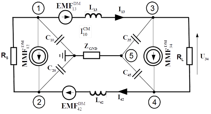
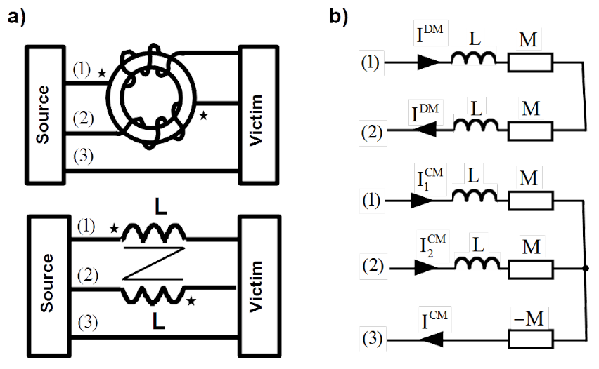
There are two contributions of symmetrical coupling with symmetrical line as shown in Fig. 5.1.
- External magnetic field of disturbance can couple with the loop built with forth and return line, between nodes 1, 3, 4 and 2. This coupling is represented with [latex]EMF_{13}^{DM}[/latex] and [latex]EMF_{42}^{DM}[/latex]. They drive current [latex]I_{sm}^{DM}[/latex] (symmetrical-magnetic) in the forth and return line.
- External electric field of disturbance can energise capacitances [latex]C_{12}[/latex] and [latex]C_{34}[/latex] between forth and return lines. This coupling is represented with [latex]MMF_{12}^{DM}[/latex] and [latex]MMF_{34}^{DM}[/latex]. They drive current [latex]I_{se}^{DM}[/latex] (symmetrical-electric) in the forth and return line.
Currents [latex]I_{sm}^{DM}[/latex] as well as [latex]I_{se}^{DM}[/latex] causes voltage drop across the load [latex]U_{34}[/latex], which overlaps the useful voltage.

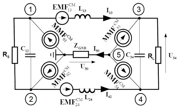
Two contributions of asymmetrical coupling with symmetrical line are possible, as shown in Fig. 5.2.
- External magnetic field of disturbance can couple with the loops built with forth line and ground reference, the first one between nodes: 1, 3, 5 and 0, the second one between nodes: 2, 4, 5 and 0. They are represented with [latex]EMF_{13}^{CM}[/latex] and [latex]EMF_{24}^{CM}[/latex].
- External electric field of disturbance can energise capacitances [latex]C_{10}[/latex], [latex]C_{20}[/latex], [latex]C_{35}[/latex] and [latex]C_{45}[/latex], each between line under consideration and the ground reference. They are represented with [latex]MMF_{10}^{CM}[/latex], [latex]MMF_{20}^{CM}[/latex], [latex]MMF_{53}^{CM}[/latex], and [latex]MMF_{54}^{CM}[/latex].
Contributions of asymmetrical coupling are harmless as long as the transmission line is perfectly balanced, in the same sense as in chapter [TCL_chapter]. Lack of balance there caused conversion of symmetrical signal to asymmetrical disturbance polluting the surrounding. Here lack of balance makes the symmetrical line sensitive to asymmetrical disturbance in which the line is immersed.
By deviation from symmetry, common mode current [latex]I_{50}[/latex] is driven in the ground reference causing longitudinal voltage drop [latex]U_{50}[/latex] across impedance [latex]Z_{GND}[/latex]. It contributes in symmetrical (transverse) voltage [latex]U_{34}[/latex] across the load.
Ratio of longitudinal voltage [latex]U_{50}[/latex] to transverse voltage [latex]U_{34}[/latex]
[latex]L_{LC} = \frac{U_{50}}{U_{34}} \hspace {2.0 cm} L_{LC(dB)} = 20 \log \left( \frac{U_{50}}{U_{34}} \right) \label{LCL}\tag{5.1}[/latex]
is called loss of longitudinal (to transverse) conversion, alternatively Longitudinal Conversion Loss LCL. It is used for rating deviation from the ideal balance by symmetrical transmission. By approaching perfect equilibrium, [latex]L_{LC}[/latex] tends to infinity.
The LCL is reciprocal to TCL introduced in chapter [TCL_chapter]. TCL quantifies lack of perfection of symmetry provoking the asymmetrical disturbance, LCL vulnerability to pick them up.
By unsymmetrical transmission any decomposition of disturbance and any protection barriers against them exist. The whole disturbance couples with them.
In order to protect the victim from the magnetomotive force appearing by electrical coupling, reasonably big capacitors mounted in parallel to the MMF must be applied. Such capacitor shortcircuits the MMF, avoiding penetration of remaining parts of the circuit. However protection from the electromotive force appearing by magnetic coupling can be realised with reasonably big inductance mounted serially to the EMF. Such inductance reduces the disturbance current in the mesh with the EMF.
Ingredients of filters
Let us consider multiconductor line as shown in Fig. 5.3 transmitting power from source to load or signal from transmitter to receiver. Occasionally this line can be a medium for disturbance propagation from source to victim. Disturbance current in each line [latex]I_i[/latex] can be decomposed into differential [latex]I_i^{DM}[/latex] and common [latex]I_i^{CM}[/latex] mode.
[latex]I_i = I_i^{DM} + I_i^{CM}[/latex]
Attribute of the components are:
- nullifying the differential mode,
- cumulation of common mode in the return path.
[latex]\sum_{i = 1}^ N I_i^{DM} = 0 \hspace {2.0 cm} I^{CM} = I_{N+1} = \sum_{i = 1}^N I_i^{CM} \label{CM_DC}\tag{5.3}[/latex]

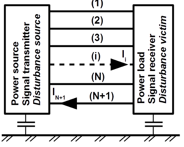
Return path can be for instance PE line by power cord or cable shield by signal transmission. However arrangements connected with the line always have some capacitances to the ground reference, as shown in Fig. 5.3. With increased frequency impedance of the return path becomes bigger than that of the return path via ground capacitances and the ground impedance, due to magnetic inductance. By such frequencies the nominal return line (N+1) must be viewed as ordinary forth lines (i = 1, 2, …, N). The multiline gains one conductor.

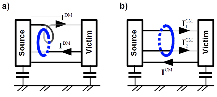
It is straightforward to separate modes one from another in two-conductors line. The target can be either individual suppression of them or quantification. As the blue ellipse in Fig. 5.4 a suppressing magnetic core or a measurement clamp can be imagined. If conductors are passed reversely through the hole in the core, as in Fig. 5.4 a) then magnetic flux excited in the core is due only to differential mode current1. In contrast to accordant passage, as in Fig. 5.4 b) which causes excitation of magnetic flux only due to common mode current.
Separation of the common mode is valid also for any muliticonductor line. However separation of differential mode is ambiguous because the differential modes build a set with number of elements depending on total number of conductors (N).

In Fig. 5.5 a) differential mode choke with three turns is presented2. As the circuit symbol either zig-zag or stars marking beginnings of the windings are used. Equivalent circuits of the choke for DM and CM currents are shown in Fig. 5.5 b). Symbol [latex]M[/latex] represents coupling inductance ([latex]M = k L[/latex]) where [latex]k[/latex] is coupling factor. By lack of leakage field ([latex]k=1[/latex]), the DM choke has inductance equal to four-tuple of the self inductance [latex]L[/latex] for the DM current and it is transparent for the CM current.

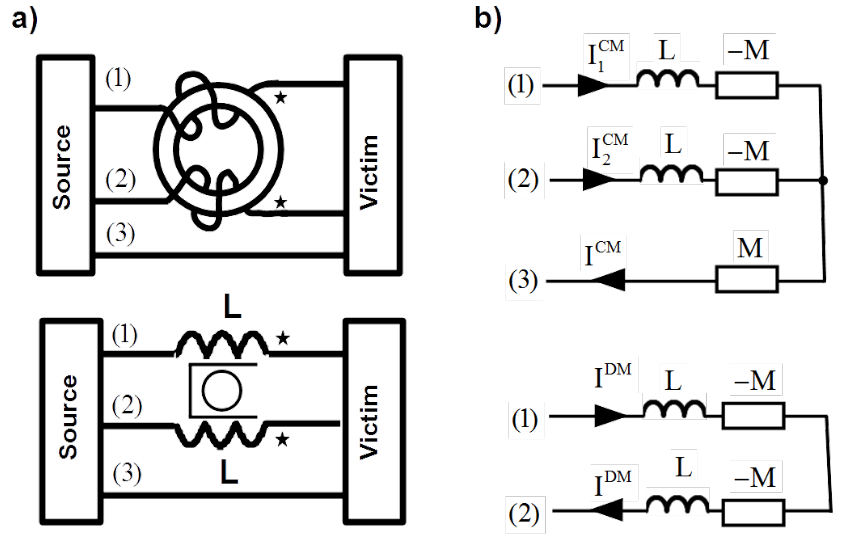
In Fig. 5.6 a) common mode choke with two turns is presented. As the circuit symbol either U-shape, circle or stars marking beginnings of the windings are used. Equivalent circuits of the choke for CM and DM currents are shown in Fig. 5.6 b). By lack of leakage field ([latex]k=1[/latex]), the CM choke has inductance equal to [latex]M[/latex] for the CM current and it is transparent for the DM current.

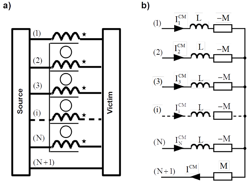
Resulting common mode inductance equal to [latex]M[/latex] is also valid for multiconductor line with arbitrary number of conductors, as shown in Fig. 5.7.
Notice that, residual current devices (RCD) commonly used in the LV electric installations as protection against electric shock are nothing else but common mode chokes mounted at all supply lines excluding PE line. They sense the residual current i.e. common mode current driven through the PE line. It is leakage current occurring only by fault. There are different sensitivity groups of RCDs depending on the broken residual current:
- high sensitivity (HS): 5 – 10 – 30 mA (for direct-contact / life injury protection),
- medium sensitivity (MS): 100 – 300 – 500 – 1000 mA (for fire protection),
- low sensitivity (LS): 3 – 10 – 30 A (typically for protection of machine).

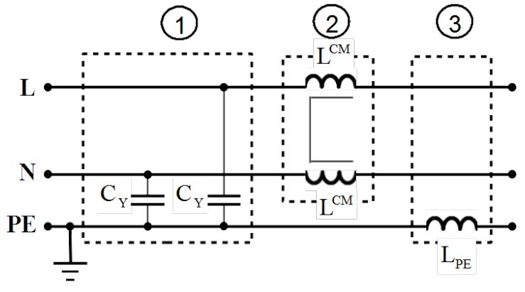
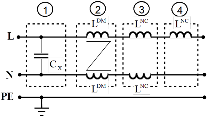
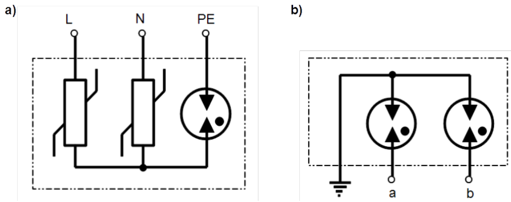
Common mode disturbance can be suppressed in the mains filter in three manners as shown exemplarily for one phase filter in Fig. 5.8, with:
- so called [latex]C_Y[/latex] capacitors mounted between each live and [latex]PE[/latex] conductor,
- common mode choke built on all live conductors,
- choke in the [latex]PE[/latex] conductor.
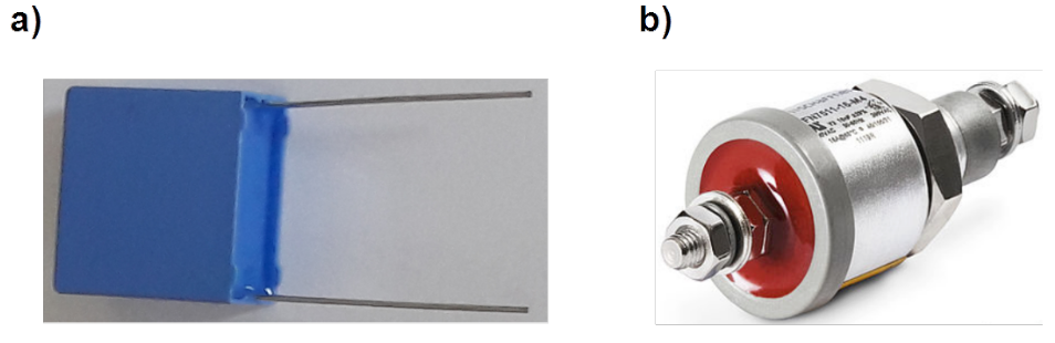
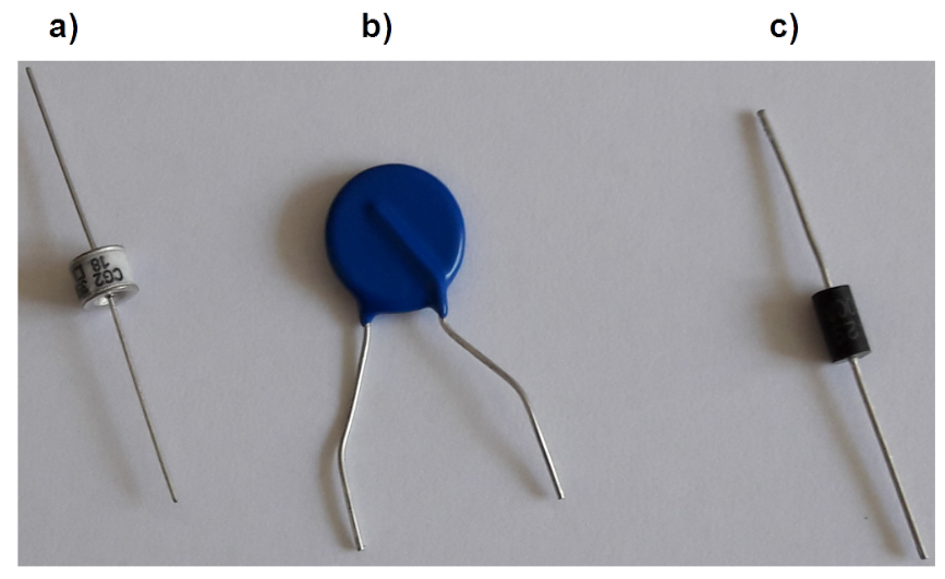
As presented in chapter [Film_cap] capacitors realised in THD technology have inductive character stating from specific frequency. From this frequency on they lose ability to shortcircuit the MMF. It is due to leads inductances, see Fig. 5.9 a). In special, costly application the feedthrough condensers are used. They do not have leads and their body has tubular or disk shape. One electrode is fed along the axis as shown in Fig. 5.9 b). Another electrode is metal cylinder with mounting collar at one end. Condenser is inserted into the hole in the metal wall between filter compartments. The collar ensures round about contact with the wall. The threaded nut screwed on the other side of the wall fixes the condenser.

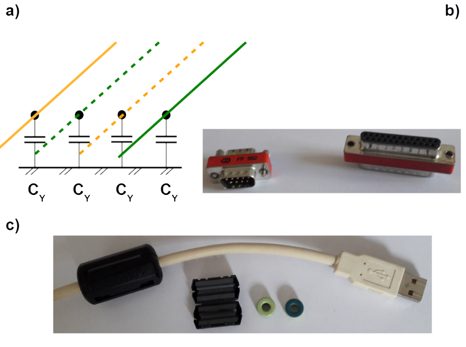
In the same way CM disturbance can be suppressed in the signal lines. Examples are gathered in Fig. 5.10.

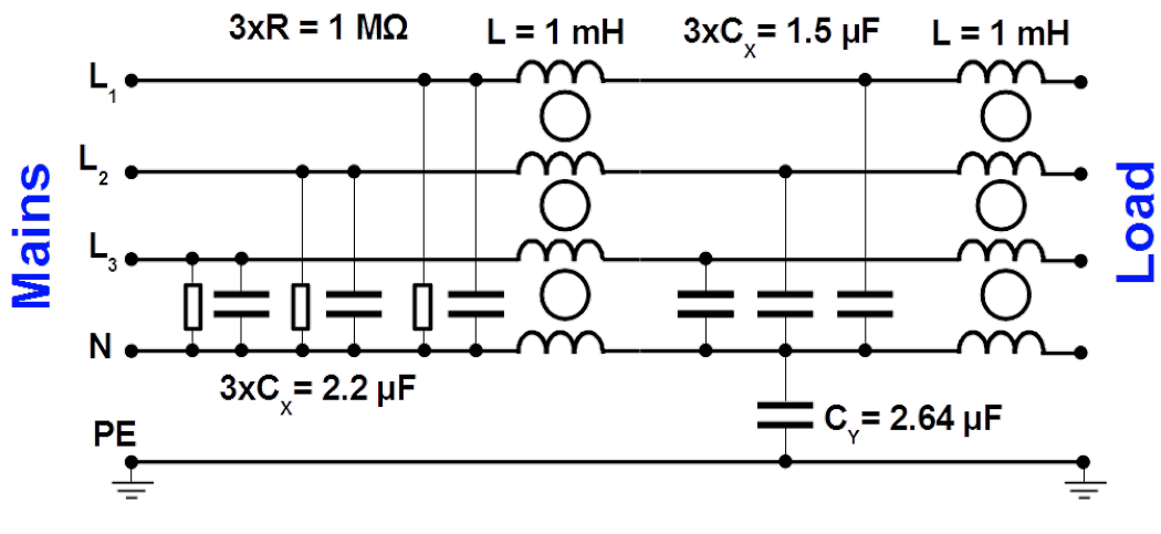
Differential mode disturbance can be suppressed in the mains filter in four manners as shown exemplarily for one phase filter in Fig. 5.11, with:
- so called [latex]C_X[/latex] capacitors mounted across the phase and neutral line,
- differential mode choke built on the phase and neutral line,
- (not coupled) chokes mounted in the phase and neutral line,
- choke mounted in either the phase or neutral line.
Measures 2 and 4 cannot be realised in the three phase filter. Moreover measure 4 is not recommended. Indeed double inductance mounted in one line can suppress differential mode alike by dividing it in both lines but this change influences in the same time relation between common and differential mode currents. Possibly it can worsen suppression of common mode.
Notice that measures for suppressing the common and differential mode support mutually one another:
- [latex]C_Y[/latex] capacitors in Fig. 5.8 build capacitance [latex]C_Y/2[/latex] across phase and neutral line thus suppresses the differential mode disturbance,
- the leakage flux of the common mode choke in Fig. 5.8 suppresses the differential mode disturbance,
- the leakage flux of the differential mode choke in Fig. 5.11 suppresses the common mode disturbance,
- (not coupled) chokes mounted in the phase and neutral line suppress as well as the common mode disturbance.
Few words are necessary about mysterious [latex]C_X[/latex] and [latex]C_Y[/latex] capacitors. Class – X and Class – Y capacitors are safety certified, whereupon the first are designed to “fail short” and the second to “fail open”. [latex]C_X[/latex] are allowed to be mounted only across the live lines because “failing short” between live line and PE could cause electrical shock hazard. Only [latex]C_Y[/latex] are allowed to be mounted between any live line and PE. Since they “fail open”, electric shock hazard is excluded. Of course [latex]C_Y[/latex] capacitors can be applied across the live lines but it is not practiced because they are more expensive then [latex]C_X[/latex] and have smaller maximal values in series. There are three subclasses of [latex]C_X[/latex] capacitors: X1, X2 and X3 and four subclasses of [latex]C_Y[/latex]: Y1, Y2, Y3 and Y4. Most common are [latex]C_{X2}[/latex] and [latex]C_{Y2}[/latex].
Why [latex]C_X[/latex] capacitors in filter shown in Fig. 5.12 are not mounted across the live lines?
Rated voltage of [latex]C_X[/latex] condensers available in the market are about [latex]310[/latex] [latex]V_{RMS}[/latex]. They do not withstand [latex]400[/latex] [latex]V_{RMS}[/latex] line to line voltage of the European mains. Therefore they are circuited in the star connected to Neutral line. Of course their attenuation is worse but alternative does not exist.
Rated voltage of [latex]C_Y[/latex] condensers available in the market are about [latex]250[/latex] [latex]V_{RMS}[/latex]. They withstand line to PE voltage of the European mains by symmetry i.e. [latex]230[/latex] [latex]V_{RMS}[/latex]. However its designed value must be raised due to unsymmetry of the load and tolerance of the mains voltage ([latex]+10\%[/latex]). Therefore they are circuited between the star point of [latex]C_X[/latex] condensers and PE line. Again their attenuation is worse but alternative does not exist.
Resistances in parallel to the [latex]C_X[/latex] condensers on the mains side of the filter accelerate discharge of [latex]C_X[/latex] by disconnecting the appliance from the mains. According to standard [@IEC-61010-1] after disconnecting the mains, voltage must decay below the active danger level within 5 s at the mains terminal and within 10 s at the remaining terminals. The active danger level is equal to 33 [latex]V_{RMS}[/latex] or 46.7 V peak value by AC voltage and 70 V DC. In humid environment these values are: 16 [latex]V_{RMS}[/latex], 22.6 V and 35 V respectively.
For value estimation of the discharge [latex]R[/latex] resistance following relations should be applied [latex]U_{Save} < U_{Max} \cdot e^{-\frac{5s}{RC}} \hspace {2 cm} R < \frac{5s}{C \cdot \ln \left(\frac{U_{Max}}{U_{Save}} \right)}[/latex] By the European mains voltage discharge resistance [latex]R = 1[/latex] [latex]M \Omega[/latex] mounted in filter in Fig. 5.12 is much smaller then the threshold value by the worst case.
Non linear suppressors
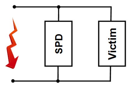
Non linear suppressors protect victims from surges described in chapter [Thunderstorm], hence the name surge protection devices SPD. They are mounted in parallel at the protected port of the device (victim)3, as shown in Fig. 5.13. Two types of protectors are used: crowbar shortcircuiting (almost) the poles of the port and clamp limiting the voltage of the pulse and sucking the surge current. The SPDs have very big impedance by normal circumstances at the port, falling to very low values by triggering i.e. when the transient exceeds the threshold.

Presentation of the SPDs here is concentrated on protection of the power AC mains ports because of importance of safety and reliability requirements.
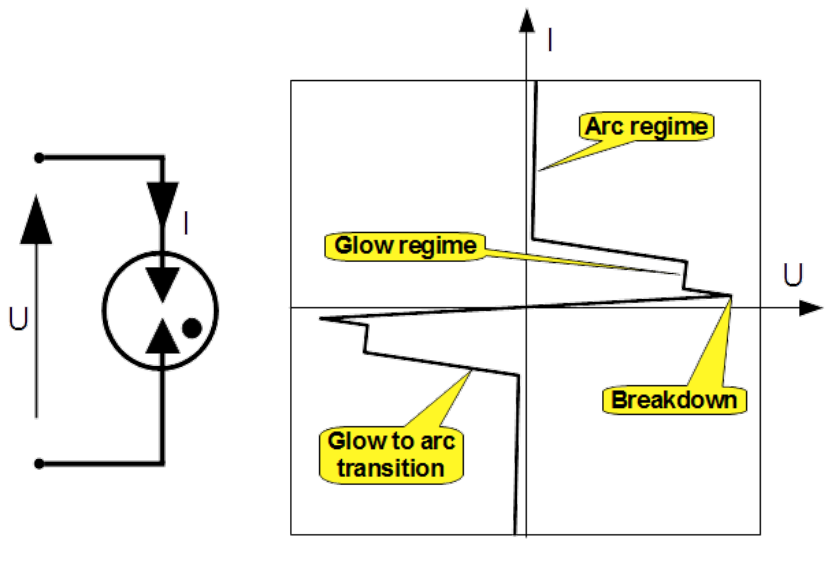
The crowbar devices are based on encapsulated gas arresters, known in abbreviation as Gas Discharge Tubes GDTs. Its [latex]I(U)[/latex] approximated characteristic is shown in Fig. 5.14. Notice that it is identical as presented in Fig. [Gas_discharge] with interchanged axes4. In normal operating conditions, called the OFF state the GDTs are very good insulators and do not contribute the leakage current. They do not shortcircuts the poles totally by ignition of the arc, called ON state because as it was demonstrated in Tab. [vapor-arc] there is little voltage across the arc, between 12 V and 17.5 V, depending on electrodes’ material. Anyway dissipation in the GDT is minimal. Therefore they can handle transients with very big energy.
Their drawback, compared with the clamp devices is longer reaction time and sustaining the arc after regress of the transient. The normal AC power conditions inhibit self-extinction of once ignited arc.
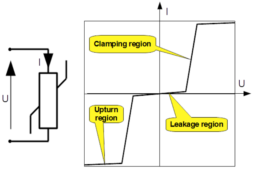
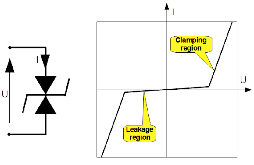
The background of clamp devices is reversely polarised semiconductor junction. Therefore clamp devices exhibits some capacitance contributing the leakage current in the OFF state. There are two types of the clamp devices: the Metal Oxide Varistors (MOVs) and Transient Voltage Suppression Diodes (TVSDs). In the ON state, they limit the voltage transient to a specific level by varying its internal resistance, see Fig. 5.15 and 5.16. They absorb the transient’s energy and therefore, cannot withstand transients with as big energy as the GDTs do. Big disadvantage of the MOVs is the "Upturn region" shown in Fig. 5.15. By very high currents their resistance increases rapidly.
The clamp devices "faults short" therefore they cannot be mounted between live lines and PE line.


| GDT | MOV | TVSD | |
|---|---|---|---|
| Response time | [latex]<1[/latex] [latex]\mu s[/latex]</td> | [latex]<100[/latex] [latex]n s[/latex]</td> | [latex]<1[/latex] [latex]n s[/latex]</td> |
| Capacitance in OFF state | [latex]<1.5[/latex] [latex]pF[/latex]</td> | [latex]180[/latex] [latex]pF[/latex] - [latex]1.7[/latex] [latex]nF[/latex] | [latex]1[/latex] [latex]nF[/latex] - [latex]11[/latex] [latex]nF[/latex] |
| Resistance in OFF state | [latex]10[/latex] [latex]G\Omega[/latex] | [latex]180[/latex] [latex]k\Omega[/latex] - [latex]900[/latex] [latex]k\Omega[/latex] | [latex]1.5[/latex] [latex]M\Omega[/latex] - [latex]22[/latex] [latex]M\Omega[/latex] |
| Trigger voltage | [latex]280[/latex] [latex]V[/latex] - [latex]7.5[/latex] [latex]kV[/latex] | [latex]130[/latex] [latex]V[/latex] - [latex]650[/latex] [latex]V[/latex] | [latex]90[/latex] [latex]V[/latex] - [latex]625[/latex] [latex]V[/latex] |
| Maximal surge current | [latex]10[/latex] [latex]kA[/latex] | [latex]10[/latex] [latex]kA[/latex] | [latex]6[/latex] [latex]kA[/latex] |
[SPD_parameters]
In Tab. 5.1 parameters of typical SPDs applicable at the AC mains port are gathered. As to time of reaction and swallowed transient energy, they decrease from left to right. GDTs and MOVs can handle merely surges while TVSDs as well BURST ([latex]5[/latex] [latex]ns[/latex] tise time) and even ESD ([latex]800[/latex] [latex]ps[/latex] tise time). The best insulation and hence the smallest leakage current ensure GDTs. At the opposite pole are TVSDs.


Combined SPDs for the one phase AC mains is presented in Fig. 5.18 a). Neither GDT is mounted between live lines nor MOVs are mounted between live lines and PE. In this way protection against electric shock is not violated.
The GDT can be mounted directly to the ground in case of telecom line, as shown in Fig. 5.18 b). [latex]48[/latex] [latex]VDC[/latex] is not capable of sustaining the arc. It extinguishes with vanishing the transient.
Shielding
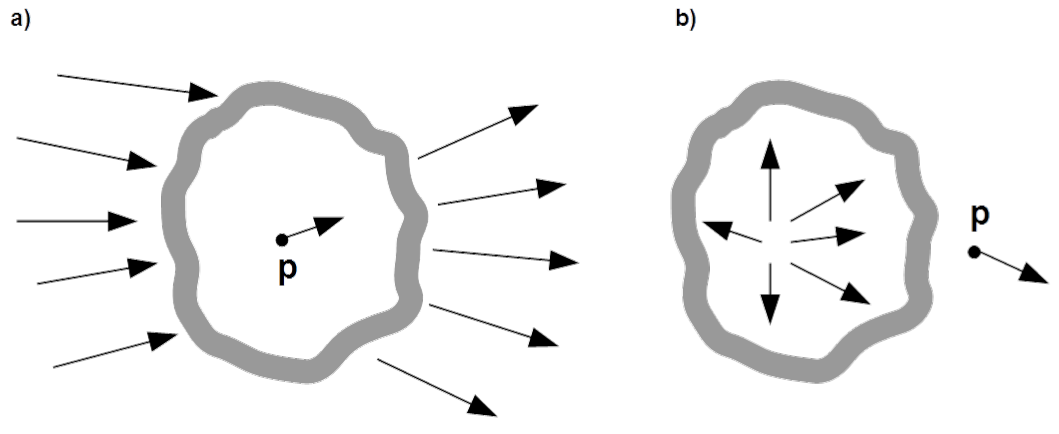
The task of a shield is to mitigate the field in the desired region. Two scenarios are possible: embracing protected region, as shown in Fig. 5.19 a) or surrounding the source of undesirable field, as shown in Fig. 5.19 b).

Constitutive formulas of shielding effectiveness are as follows [latex]\begin{array}{rclrcl} SE^E(p) & = & \frac{\left |\overrightarrow{E_0}(p) \right |}{\left |\overrightarrow{E_S}(p)\right |} & \hspace{1cm} SE^E_{dB}(p) & = & 20 \log \left( \frac{\left |\overrightarrow{E_0}(p) \right |}{\left |\overrightarrow{E_S}(p) \right |} \right) \\ \\ SE^H(p) & = & \frac{ \left |\overrightarrow{H_0}(p) \right |}{\left |\overrightarrow{H_S}(p) \right |} & \hspace{1cm} SE^H_{dB}(p) & = & 20 \log{ \left( \frac{\left |\overrightarrow{H_0}(p) \right |}{\left |\overrightarrow{H_S}(p) \right|} \right)} \label{SE_EH} \end{array}\tag{5.5}[/latex]
These formulas are the ratios of absolute values of the fields [latex]E_0(p)[/latex] or [latex]H_0(p)[/latex] in point [latex]p[/latex] of interest without the shield and fields [latex]E_S(p)[/latex] or [latex]H_S(p)[/latex] in the same point [latex]p[/latex] after immersing the shield.
Mind that shielding effectiveness is defined in the same way as attenuation of a two-port described in chapter [Attenuation]. Field strength in the point of interest is determined in two situation: by direct exposition to the sinner and by inserting in-between the shield. Later it will be shown that shielding effectiveness is also referred to some medium quantity like attenuation to the reference impedance.
Static and quasi-static fields
Metal shields
If separated, source charge e.g. [latex]+Q[/latex], as shown in Fig. 5.20 is enclosed in the metallic compartment5, then surrounding is not free of its electric field, unless the enclosure is grounded. Free electrons in metal are attracted by the free source charge inside, causing excess of positive charges at the outer surface of the enclosure. It does not matter whether the free source charge is placed centrically or eccentrically as shown in Fig. 5.20 a) and b) respectively. Electric flux over arbitrary closed surface [latex]S[/latex] is related to the net free charges [latex]\sum Q[/latex] enclosed in the integration surface with the Gauss’s theorem
[latex]\unicode{x222F}_S\overrightarrow{D}\cdot \overrightarrow{dS} = \sum Q[/latex]
where [latex]\overrightarrow{D}[/latex] is vector of electric flux density.
In both cases the net charge is equal to the source [latex]+Q[/latex] charge. Consequently [latex]SE_{E_{dB}}(p) = 0[/latex] dB.

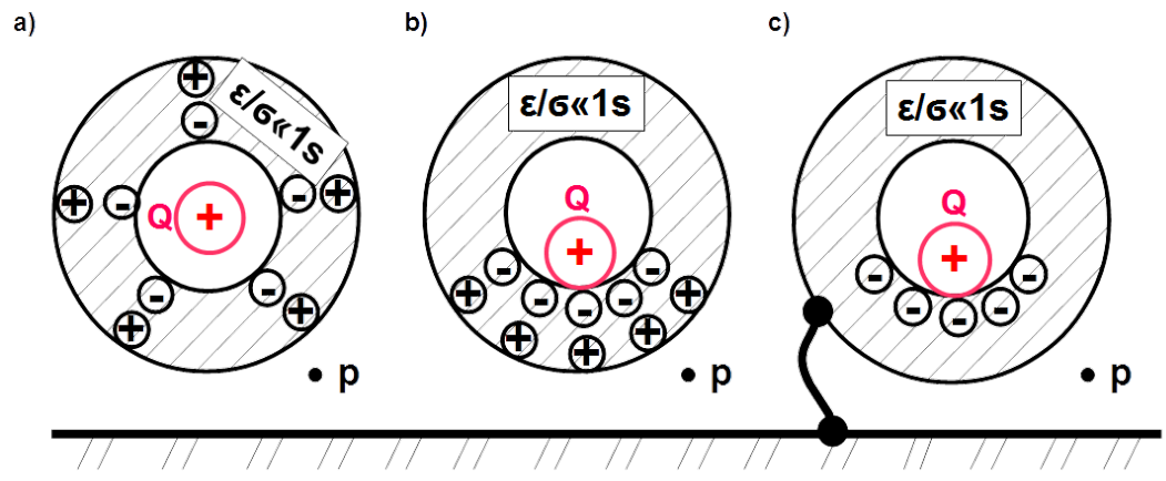
By grounding the enclosure, as shown in n Fig. 5.20 c) free electrons are brought from the most distant region of the ground, leaving free of charge the outer surface of the enclosure and causing [latex]SE^E_{dB} (p) \to \infty[/latex] dB . Free charges in conductor seek to get away from each other as far as possible leaving the inside free of electric field.

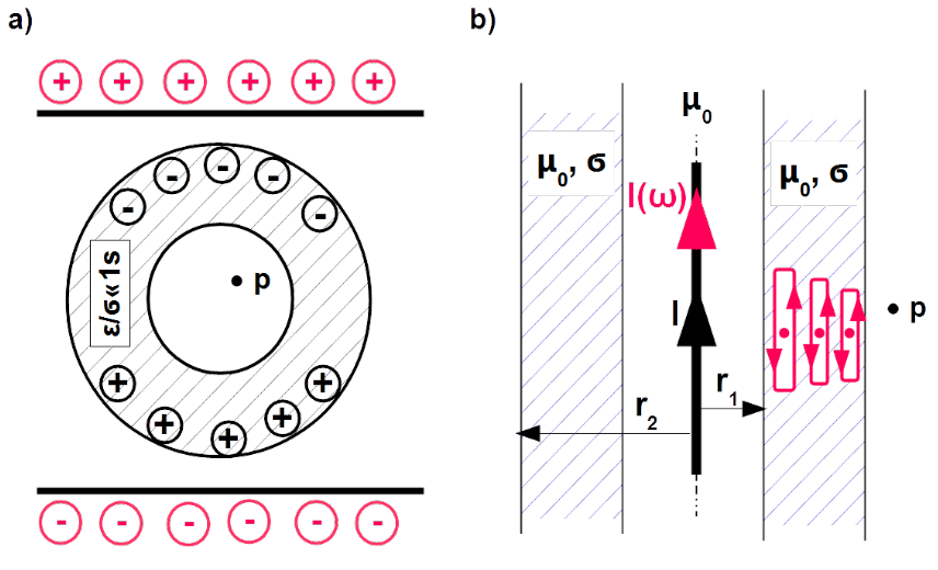
In the same way the case shown in Fig. 5.21 a) can be rationalised. Voltage is maintained between two horizontal metal plates. This results in charging one plate positively and another negatively with the same quantity of charge. Free electrons are attracted by the positive charges concentrated at the upper metal plate from the most remote regions of enclosure. Consequently the same quantity of positive and negative charges are concentrated only at the outer surface of the enclosure liberating the inside from the field.
Rules valid for electrostatic fields are in force in case of extremely low or quasi-static electric fields.
As to magnetic properties of materials there are two origins of it. Atoms have magnetic moment quantified with Eq.([m_dipole]), due to circular movement of electrons around nucleus. Moreover, electrons besides electric charge have the property of spin about their own axes. In other words, electrons possess an intrinsic magnetic dipole moment6 [@Hammond_2]. In most materials these magnetic moments almost cancels each other. Their relative permeability [latex]\mu_r[/latex] is almost equal one, whereat [latex]\mu_r < 1[/latex] by diamagnetics and [latex]\mu_r > 1[/latex] by paramagnetics. Diamagnetics subjected to an external magnetic field reduces resulting field whereat magnetic moments in paramagnetic materials turn in direction to strengthen the incident field. Ferromagnetics are paramagnetics with very strong amplification attribute.
Magnetic field of conducted currents is ruled with the Ampère’s circular theorem which couples strength of magnetic field [latex]\overrightarrow{H}[/latex] with net conducted current [latex]I[/latex] embraced with the integration perimeter [latex]l[/latex]
[latex]\oint_l \overrightarrow{H}\cdot \overrightarrow{dl} = \sum I[/latex].
In Fig. 5.21 b) infinitely long cylindrical structure is shown. Conductor driving constant current [latex]I[/latex] is layouted along the axis. It is source of azimuthal magnetic field according to the Ampère’s circular theorem. Nothing changes if conductor is immersed in the paramagnetic or diamagnetic metal cylinder ([latex]\mu_r = 1[/latex]) with inner and outer radius [latex]r_1[/latex] and [latex]r_2[/latex] respectively. The net conducted current remains unchanged i.e. shied effectiveness is zero.
Situation changes if the current is alternated [latex]I(\omega)[/latex] as presented with the red arrow in Fig. 5.21 b). Magnetic induction [latex]\overrightarrow{B}(\omega)[/latex] is source of eddy currents in the shield material. Nature of eddy currents is conduction. They can be depicted with small loops distributed in the whole cross section of the shield (red contours). Overlapping of current’s loops results with inhomogeneous distribution of the longitudinal current density in the shield. This reduces net current present in the Ampère’s theorem.
The inhomogeneous current distribution and in consequence shielding effectiveness depends on relation between skin depth defined with formula Eq.([delta]) and thickness of the shield. The smaller this relation, the bigger shielding effectiveness. In extreme case skin depth tends to zero, volume current becomes surface current on the inner surface of the shield liberating the shield material and space outside the shield from magnetic field.
On the opposite pole is situation by very thin shield compared to the skin depth. Then the sense of the current density at the outer surface of the shield is opposite to that at the inner surface. Resulting induced current, applied in the Ampère’s circular theorem is almost zero and shield effectiveness is minimal.
Skin depth by [latex]50[/latex] [latex]Hz[/latex] in copper, aluminium and brass are [latex]\delta_{Cu} \approx 9[/latex] [latex]mm[/latex], [latex]\delta_{Al} \approx 1.2[/latex] [latex]cm[/latex] and [latex]\delta_{Brass} \approx 1.8[/latex] [latex]cm[/latex]. By iron with [latex]\mu_r = 1000[/latex] it is [latex]\delta_{Fe} \approx 0.7[/latex] [latex]mm[/latex]. The engineer’s rule of thumb i.e. [latex]1/10[/latex] suggests effective shielding by [latex]50[/latex] [latex]Hz[/latex] with shield thickness between [latex]10[/latex] [latex]cm[/latex] and [latex]20[/latex] [latex]cm[/latex] applying copper, aluminium or brass respectively and [latex]7[/latex] [latex]cm[/latex] by iron shield.
One example of such shielding is copper foil or tape wrapped over the pulse transformer of Switched Mode Power Supplier. Such transformers operate with frequencies from tenth of [latex]kHz[/latex] up to over 100 [latex]kHz[/latex]. Wrapping is the only measure protecting the surrounding on the PCB from direct magnetic coupling.
Computer era of monitors based on electron guns in which electron beam is deflected with low frequency magnetic field is over. At that time operation of monitors for example in offices located by railway stations with electrical traction was possible only with placing monitors in mu-metal or permalloy covers. Their relative permeability [latex]\mu_r[/latex] by [latex]1[/latex] [latex]kHz[/latex] are [latex]30'000[/latex] and [latex]80'000[/latex] respectively. The same concerned TV sets and oscilloscopes with electron guns.
Shielding of alternated magnetic field due to eddy currents can be interpreted with energy conservation. Energy of the source current [latex]I(\omega)[/latex] is dissipated in the conducting material, decreasing energy bound in magnetic field. The reference quantity for shielding effectiveness is the shin depth. Memorise, that grounding of the shield, unlike by static electric field has any influence on the effectiveness.
Shielding with diamagnetics and ferromagnetics
If separated, source charge e.g. [latex]+Q[/latex], as shown in Fig. 5.22 is enclosed in the dielectric compartment, then surrounding is not free of its electric field. Electric dipoles inside the enclosure, either induced or permanent turns in the direction to weaken the source field inside the dielectric. In consequence negative charge appears at the internal surface of dielectric and positive at the eternal surface. Anyway the net charge remains unchanged [latex]+Q[/latex] causing zero effectiveness of shielding. It is independent on the shape of the enclose as shown in Fig. 5.22 a) and b).

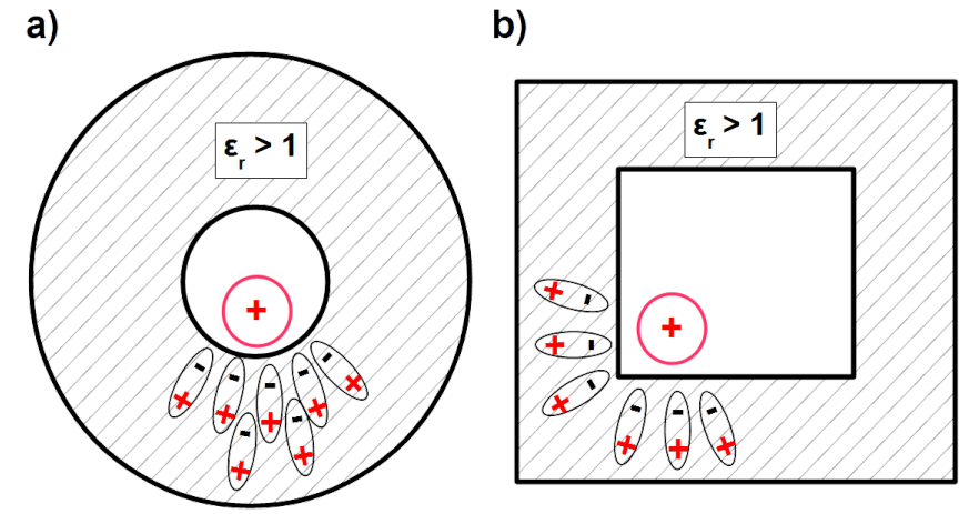
If between two charged metal plates oriented horizontally as shown in Fig. 5.21 a) dielectric cylinder is inserted as shown in Fig. 5.23 a) then electric field inside cylinder is mitigated. There is twofold representation of field strength vector [latex]\overrightarrow{E}[/latex] in the figure7. One is set of streamlines, another is colours’ visualization of the vector magnitude.
Dielectric material which weakens the incident field of free charges "expels" the field from the inside. The strongest field depicted with bright tones is around the cylinder. Cylinder itself and its interior are dark. Presented example is calculated by [latex]\epsilon_r = 10[/latex]. Shielding effectiveness inside was [latex]SE_E(p) \approx 7.5[/latex] [latex]dB[/latex]. Noticeable is dielectric permittivity [latex]\epsilon[/latex] as reference by shielding effectiveness of electric field.

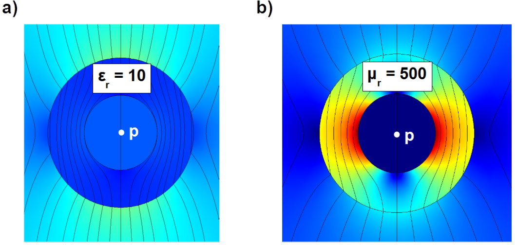
Imagine two metal bars oriented vertically, driving constant current one forth, another back. Between the bars homogeneous magnetic field is established. If between the bars ferromagnetic cylinder is inserted as shown in Fig. 5.23 b) then magnetic field inside cylinder is mitigated. There is twofold representation of vector of magnetic flux density [latex]\overrightarrow{B}[/latex] in the figure8. One is set of streamlines, another is colours’ visualization of the vector magnitude.
Ferromagnetic material which strengthens the incident field of conducted currents in the bars "attracts" the field to the inside. The strongest field depicted with bright tones is inside the cylinder. Cylinder exterior and interior are dark. Presented example is calculated by [latex]\mu_r = 500[/latex]. Shielding effectiveness inside was [latex]SE^H(p) \approx 40[/latex] [latex]dB[/latex].
Measurement of static magnetic fields with probes is always preceded with compensation (calibration) procedure. It consists in simulating conditions liberating from any static magnetic field. For this, the field sensor is placed in the ferromagnetic cylinder with bottom in order to eliminate influence of the Earth magnetic field.
Noticeable is magnetic permeability [latex]\mu[/latex] as reference by shielding effectiveness of magnetic field.
RF shielding in the far field zone

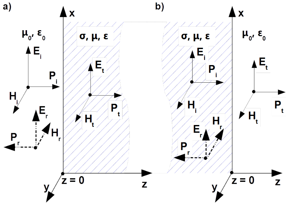
If the incident plane (TEM) wave [latex]\overrightarrow{{\bf E}}_i[/latex], [latex]\overrightarrow{{\bf H}}_i[/latex] propagates in z-direction in the lossless medium [latex]\mu_0[/latex], [latex]\epsilon_0[/latex] as shown in Fig. 5.24 a) then
[latex]\begin{array}{rclcl} \overrightarrow{{\bf E}}_i (z) & = & {\bf{E}}_m e^{-j\beta_0 z} \cdot \overrightarrow{1}_x & = & {Z_0} {\bf{H}}_m e^{-j\beta_0 z} \cdot \overrightarrow{1}_x \\ \\ \overrightarrow{\bf{H}}_i (z) & = & \frac{{\bf{E}}_m }{{Z_0}} e^{-j\beta_0 z} \cdot \overrightarrow{1}_y & = & {\bf{H}}_m e^{-j\beta_0 z} \cdot \overrightarrow{1}_y \label{EH_incident} \end{array}\tag{5.24}[/latex]
where [latex]Z_0[/latex] is intrinsic impedance defined in Eq. ([Z_0]) and [latex]\beta_0[/latex] is phase constant defined in Eq. ([beta]).
Vector product of these vectors gives the Poynting vector [latex]\overrightarrow{{\bf P}}_i(z)[/latex] oriented along the z-axis.
[latex]\overrightarrow{{\bf P}}_i(z)=\overrightarrow{{\bf E}}_i(z) \times \overrightarrow{\bf{H}}_i(z) \label{P_incident} \tag{5.9}[/latex]
If such plane (TEM) wave impinges on a lossy medium [latex]\sigma[/latex], [latex]\mu[/latex], [latex]\epsilon[/latex] tangential to the wavefront, by [latex]z = 0[/latex] as shown in Fig. 5.24 a) then part of the field is reflected and travels backwards. These fields have subscripts [latex]r[/latex]. Analogue to the voltage and current reflection coefficients in the circuit theory, presented in chapter [impedance maching], Eq. ([GAMMA_2]) and Eq. ([GAMMA_4]) respectively, reflection coefficients [latex]{\bf \Gamma}^E[/latex] and [latex]{\bf \Gamma}^H[/latex] for electric and magnetic field at the boundary are introduced
[latex]{\bf \Gamma}^E = \left | \frac{ \overrightarrow{\bf{ E}}_r }{ \overrightarrow{\bf{ E}}_i } \right | \hspace{1.5cm} {\bf \Gamma}^H = - \left | \frac{ \overrightarrow{{\bf H}}_r }{ \overrightarrow{ {\bf H}}_i } \right | \label{Gamma_1}\tag{5.18a}[/latex]
along with transmission coefficients [latex]{\bf T}^E[/latex] and [latex]{\bf T}^H[/latex]
[latex]{\bf T}^E = \left| \frac{ \overrightarrow{\bf{ E}}_t }{ \overrightarrow{\bf{ E}}_i } \right| \hspace{1.5cm} {\bf T}^H = \left| \frac{ \overrightarrow{{\bf H}}_t }{ \overrightarrow{ {\bf H}}_i } \right| \label{Gamma_1_}\tag{5.18b}[/latex]
These coefficients concerns phasors [latex]{\bf{ E}}[/latex] and [latex]{\bf{ H}}[/latex] for vector’s senses according to Fig. 5.24 a).
[latex]\begin{array}{rclcl} \overrightarrow{{\bf E}}_r (z) & = & {\bf \Gamma}^E {\bf{E}}_m e^{j\beta_0 z} \cdot \overrightarrow{1}_x & = & - {Z_0} {\bf \Gamma}^H {\bf{H}}_m e^{j\beta_0 z} \cdot \overrightarrow{1}_x \\ \\ \overrightarrow{\bf{H}}_r (z) & = & - \frac{{\bf \Gamma}^E {\bf{E}}_m }{{Z_0}} e^{j\beta_0 z} \cdot \overrightarrow{1}_y & = & {\bf \Gamma}^H {\bf{H}}_m e^{j\beta_0 z} \cdot \overrightarrow{1}_y \label{EH_refl} \end{array}\tag{5.12}[/latex]
The rest is transmitted to the lossy medium. These fields have subscripts [latex]t[/latex]. Transmission coefficients [latex]{\bf T}^E[/latex] and [latex]{\bf T}^H[/latex] denotes amount of transmitted fields
[latex]\begin{array}{rclcl} \overrightarrow{{\bf E}}_t (z) & = & {\bf T}^E {\bf{E}}_m e^{-{\bf \gamma} z} \cdot \overrightarrow{1}_x & = & {\bf Z} {\bf T}^H {\bf{H}}_m e^{-{\bf \gamma} z} \cdot \overrightarrow{1}_x \\ \\ \overrightarrow{\bf{H}}_t (z) & = & \frac{{\bf T}^E {\bf{E}}_m }{{\bf Z}} e^{-{\bf \gamma} z} \cdot \overrightarrow{1}_y & = & {\bf T}^H {\bf{H}}_m e^{-{\bf \gamma} z} \cdot \overrightarrow{1}_y \label{EH_trans} \end{array}\tag{5.25}[/latex]
where
[latex]{\bf{\gamma }} = \sqrt{j \omega \mu (\sigma + j \omega \epsilon)} = \alpha + j \beta \label{Propagation}\tag{5.14}[/latex]
is propagation constant in the lossy medium which is composed of attenuation coefficient [latex]\alpha[/latex] and phase constant [latex]\beta[/latex].
[latex]{\bf Z}[/latex] is intrinsic impedance of the lossy medium
[latex]{\bf Z} = \sqrt{ \frac{j \omega \mu}{ \sigma + j \omega \epsilon}} \label{Z}\tag{5.15}[/latex]
Continuity of tangential component of the electric field at the interface [latex]z = 0[/latex]
[latex]\begin{array}{rclrcl} 1 + {\bf \Gamma}^E & = & {\bf T}^E \hspace{2cm} & Z_0 \left( 1 - {\bf \Gamma}^H \right ) & = & {\bf Z} {\bf T}^H \end{array} \label{Gamma_T1}\tag{5.16}[/latex]
along with continuity of tangential component of the magnetic field at the interface [latex]z = 0[/latex] yields
[latex]\begin{array}{rclrcl} {\bf Z} \left( 1 - {\bf \Gamma}^E \right ) & = & Z_0 {\bf T}^E \hspace{2cm} & 1 + {\bf \Gamma}^H & = & {\bf T}^H \end{array} \label{Gamma_T2}\tag{5.17}[/latex]
yields
[latex]{\bf \Gamma}^E = \frac{{\bf Z} - Z_0 }{{\bf Z} + Z_0} \hspace{1.5cm} {\bf \Gamma}^H = \frac{Z_0 - {\bf Z} }{Z_0 + {\bf Z}} \label{Gamma_1nnn}\tag{5.18}[/latex]
For the sake of convenience only [latex]{\bf \Gamma}^E[/latex] will be used with omitted superscript
[latex]{\bf \Gamma} = {\bf \Gamma}^E = - {\bf \Gamma}^H = \frac{{\bf Z} - Z_0 }{{\bf Z} + Z_0} \label{Gamma_2}\tag{5.19}[/latex]
Transmission coefficients are as follows
[latex]\begin{array}{rclrclrcl} {\bf T}^E & = & 2 \frac{ {\bf Z}} {{\bf Z} + Z_0} \hspace{1cm} & {\bf T}^H & = & 2 \frac{ Z_0 } {{\bf Z} + Z_0} \hspace{1cm} & Z_0 {\bf T}^E & = & {\bf Z} {\bf T}^H\\ \label{TE_1} \end{array}\tag{5.20}[/latex]
In most cases shields are constructed from materials in which density of displacement current is negligible small compared to conducted current by frequency of interest9 ([latex]\sigma \gg \omega \epsilon[/latex]) then propagation constant, defined with Eq. (5.14) simplifies
[latex]{\bf{\gamma }} = \alpha + j \beta = (1 + j)\sqrt{\frac{\omega \mu \sigma}{2}} = (1 + j) \frac{1}{\delta} \label{Propagation_2}\tag{5.21}[/latex]
Compare with Eq. ([delta]).
Intrinsic impedance defined with Eq. (5.15) simplifies as follows
[latex]{\bf Z} = (1 + j)\sqrt{\frac{\omega \mu }{2 \sigma}} = (1 + j) \frac{1}{ \sigma \delta} = \sqrt{\frac{\omega \mu }{ \sigma}} e^{j \frac{\pi}{4}} \label{Z_2}\tag{5.22}[/latex]
Notice that propagation constant [latex]\bf \gamma[/latex] as well as intrinsic impedance [latex]\bf Z[/latex] increases proportionally to square root of frequency.
Remarkable is very small value of intrinsic impedance by well conducting metals. For aluminium and copper its module is smaller than [latex]70[/latex] [latex]m\Omega[/latex] and [latex]60[/latex] [latex]m\Omega[/latex] respectively by [latex]40[/latex] [latex]GHz[/latex].
If the lossless medium is vacuum with intrinsic impedance [latex]Z_0 = 377[/latex] [latex]\Omega[/latex] and lossy medium is well conducting metal, then [latex]{\bf{Z}} \ll Z_0[/latex] and [latex]{\bf \Gamma} \approx -1[/latex]. It mean that electric field is almost totally reflected because [latex]\overrightarrow{\bf{ E}}_r \approx -\overrightarrow{\bf{ E}}_i[/latex] but magnetic field is nearly doubled since [latex]{\bf T}^H = 1 - {\bf \Gamma} \approx 2[/latex]. Analogy to line with distributed parameters, terminated with the shortcircuit is obvious.
If the incident plane (TEM) wave [latex]\overrightarrow{{\bf E}}_i[/latex], [latex]\overrightarrow{{\bf H}}_i[/latex] propagates in z-direction in the lossy medium [latex]\sigma[/latex], [latex]\mu[/latex], [latex]\epsilon[/latex] as shown in Fig. 5.24 b) then
[latex]\begin{array}{rclcl} \overrightarrow{{\bf E}}_i (z) & = & {\bf{E}}_m e^{-{\bf \gamma} z} \cdot \overrightarrow{1}_x & = & {\bf Z} {\bf{H}}_m e^{-{\bf \gamma} z} \cdot \overrightarrow{1}_x \\ \\ \overrightarrow{\bf{H}}_i (z) & = & \frac{{\bf{E}}_m }{{\bf Z}} e^{-{\bf \gamma} z} \cdot \overrightarrow{1}_y & = & {\bf{H}}_m e^{-{\bf \gamma} z} \cdot \overrightarrow{1}_y \label{EH_incident_a} \end{array}\tag{5.24}[/latex]
By reaching the outlet surface to the lossless medium tangential to the wavefront by [latex]z = 0[/latex] as shown in Fig. 5.24 b), part of the field is reflected and travels backwards. These fields have subscripts [latex]r[/latex].
[latex]\begin{array}{rclcl} \overrightarrow{{\bf E}}_r (z) & = & {\bf \Gamma}^E {\bf{E}}_m e^{{\bf \gamma} z} \cdot \overrightarrow{1}_x & = & - {\bf Z} {\bf \Gamma}^H {\bf{H}}_m e^{{\bf \gamma} z} \cdot \overrightarrow{1}_x \\ \\ \overrightarrow{\bf{H}}_r (z) & = & - \frac{{\bf \Gamma}^E{\bf{E}}_m }{{\bf Z}} e^{{\bf \gamma} z} \cdot \overrightarrow{1}_y & = & {\bf \Gamma}^H {\bf{H}}_m e^{{\bf \gamma} z} \cdot \overrightarrow{1}_y \label{EH_incident_b} \end{array}\tag{5.24}[/latex]
The rest is transmitted to the lossless half infinite medium
[latex]\begin{array}{rclcl} \overrightarrow{{\bf E}}_t (z) & = & {\bf T}^E {\bf{E}}_m e^{-j\beta_0 z} \cdot \overrightarrow{1}_x & = & Z_0 {\bf T}^H {\bf{H}}_m e^{-j\beta_0 z} \cdot \overrightarrow{1}_x \\ \\ \overrightarrow{\bf{H}}_t (z) & = & \frac{{\bf T}^E {\bf{E}}_m }{Z_0} e^{-j\beta_0 z} \cdot \overrightarrow{1}_y & = & {\bf T}^H {\bf{H}}_m e^{-j\beta_0 z} \cdot \overrightarrow{1}_y \end{array}\tag{5.25}[/latex]
Proceeding in the same manner as in case shown in Fig. 5.24 a) following relations can be derived
[latex]{\bf \Gamma} = {\bf \Gamma}^E = - {\bf \Gamma}^H = \frac{Z_0 - {\bf Z} }{Z_0 + {\bf Z}} \label{Gamma_3}\tag{5.26}[/latex]
Transmission coefficients are as follows
[latex]\begin{array}{rclrclrcl} {\bf T}^E & = & 2 \frac{Z_0 } {Z_0 + {\bf Z}} \hspace{1cm} & {\bf T}^H & = & 2 \frac{ {\bf Z} } {Z_0 + {\bf Z}} \hspace{1cm} & {\bf Z} {\bf T}^E & = & Z_0 {\bf T}^H\\ \label{TE_2} \end{array}\tag{5.27}[/latex]
Noticeable is the case when the lossy medium is well conducting metal with much smaller intrinsic impedance [latex]{\bf{Z}}[/latex] then intrinsic impedance of the lossless vacuum [latex]{\bf{Z}} \ll Z_0 = 377[/latex] [latex]\Omega[/latex]. Then [latex]{\bf \Gamma} \approx 1[/latex]. It mean that electric field is nearly doubled [latex]{\bf T}^E = 1 + {\bf \Gamma} \approx 2[/latex] but magnetic field is nearly extinguished [latex]\overrightarrow{\bf{ H}}_r \approx -\overrightarrow{\bf{ H}}_i[/latex]. Similar as by the line with distributed parameters terminated with the opencircuit.
If shielding barrier has finite thickness [latex]d[/latex] then inside the shield two waves are traveling: forwards [latex]\overrightarrow{\bf{ E}}_{12}(z)[/latex], [latex]\overrightarrow{\bf{ H}}_{12}(z)[/latex] from boundary [latex]1[/latex] to [latex]2[/latex] and backwards [latex]\overrightarrow{\bf{ E}}_{21}(z)[/latex], [latex]\overrightarrow{\bf{ H}}_{21}(z)[/latex] from boundary [latex]2[/latex] to [latex]1[/latex] as shown in Fig. 5.25. Behind the shield the rest of field [latex]\overrightarrow{\bf{ E}}_{t}(z)[/latex], [latex]\overrightarrow{\bf{ H}}_{t}(z)[/latex] propagates reflection free
[latex]\begin{array}{lcllcl} \overrightarrow{\bf{ E}}_{12} (z) & = & {\bf{ E}}_{12}(0) e^{-{\bf \gamma} z} \overrightarrow{1}_x \hspace{0.4cm} & \overrightarrow{\bf{ E}}_{21} (z) & = & {\bf{ E}}_{12} (0) e^{{\bf \gamma} z} \overrightarrow{1}_x \\ \\ \overrightarrow{\bf{ H}}_{12} (z) & = & \frac{{\bf{ E}}_{12}(0)}{{\bf Z}} e^{-{\bf \gamma} z} \overrightarrow{1}_y \hspace{0.4cm} & \overrightarrow{\bf{ H}}_{21} (z) & = & - \frac{{\bf{ E}}_{21}(0)}{{\bf Z}} e^{{\bf \gamma} z} \overrightarrow{1}_y \\ \\ \overrightarrow{\bf{ E}}_{t} (z) & = & {\bf{ E}}_{t}(d) e^{-j{\bf \beta_0} (z-d)} \overrightarrow{1}_x \hspace{0.4cm} & \overrightarrow{\bf{ H}}_{t} (z) & = & \frac{{\bf{ E}}_{t}(d)}{Z_0} e^{-j{\bf \beta_0} (z-d)} \overrightarrow{1}_y \end{array}[/latex]

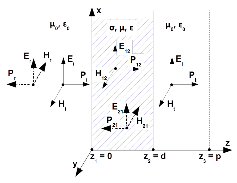
Continuity of tangential component of the electric field at the boundary [latex]z = 0[/latex] and [latex]z = d[/latex]
[latex]{\bf E}_i (0) + {\bf E}_r (0) = {\bf E}_{12} (0) + {\bf E}_{21} (0)[/latex]
[latex]\nonumber[/latex]
[latex]{\bf E}_{12} (0) e^{-{\bf \gamma} d} + {\bf E}_{21} (0) e^{{\bf \gamma} d}= {\bf E}_t (d) \label{E_tang} \tag{5.30}[/latex]
along with continuity of tangential component of the magnetic field at the boundary [latex]z = 0[/latex] and [latex]z = d[/latex]
[latex]\frac{{\bf E}_i (0)}{Z_0} - \frac{{\bf E}_r (0)}{Z_0} = \frac{{\bf E}_{12}(0)}{\bf Z} - \frac{{\bf E}_{21}(0)}{\bf Z}[/latex]
[latex]\nonumber[/latex]
[latex]\frac{{\bf E}_{12}(0)}{\bf Z} e^{-{\bf \gamma} d} - \frac{{\bf E}_{21}(0)}{\bf Z} e^{{\bf \gamma} d}=\frac{ {\bf E}_t(d) }{Z_0} \label{H_tang} \tag{5.32}[/latex]
gives the ratio of incident wave at the interface [latex]z_1 = 0[/latex] and transmitted wave at the interface [latex]z_2 = d[/latex] [@Clayton]
[latex]\frac{{\bf E}_i (0)}{{\bf E}_t(d)} = \frac{ \left( Z_0 + {\bf Z} \right)^2 } {4 Z_0 {\bf Z}} \left[ 1- \left(\frac{Z_0 - {\bf Z} }{Z_0 + {\bf Z}} \right)^2 e^{-2 {\bf{\gamma }} d} \right] e^{{\bf \gamma } d} \label{RF_SE_n}\tag{5.33}[/latex]
Shielding effectiveness of electric field due to Eq.(5.21) yields10
[latex]SE^E (p) = \left | \frac{{\bf E}_i(p)}{{\bf E}_t(p)} \right | = \left | \frac{{\bf E}_i (0)}{{\bf E}_t(d)} \right | = \left |\frac{ \left( Z_0 + {\bf Z} \right)^2 } {4 Z_0 {\bf Z}} \right | \cdot \left | 1- \left(\frac{Z_0 - {\bf Z} }{Z_0 + {\bf Z}} \right)^2 e^{-2 {\bf{\gamma }} d} \right | e^{\frac{d}{ \delta}} \label{RF_SE_m}\tag{5.34}[/latex]
Let’s derive transmitted field due to single forward passage through barrier. By impinging the barrier by [latex]z_1 = 0[/latex] transmitted is part of the incident field [latex]{\bf {E}_i(0)}[/latex] according to transmission coefficient [latex]{\bf T}^E[/latex] presented in Eq. (5.20)
[latex]{\bf E}_{{12}_1}(0) = {\bf T}^E {\bf E}_i(0) = \frac{2 {\bf Z} } {Z_0 + {\bf Z}} {\bf E}_i(0) \label{E12_10}\tag{5.35}[/latex]
This field by reaching the interface of the barrier by [latex]z_2 = d[/latex] is attenuated by the exponential function [latex]e^{-{\bf{\gamma }} d}[/latex]
[latex]{\bf E}_{{12}_1}(d) = \frac{2 {\bf Z} } {Z_0 + {\bf Z}} e^{-{\bf{\gamma }} d } {\bf E}_i(0) \label{E12_1d}\tag{5.36}[/latex]
Part of the field according to transmission coefficient [latex]{\bf T}^E[/latex] presented in Eq. (5.27) leaves the barrier
[latex]{\bf E}_{t_1} (d)= {\bf T}^E {\bf E}_{{12}_1}(d) = \frac{2 Z_0 } {Z_0+ {\bf Z}} \cdot \frac{2 {\bf Z} } {Z_0+ {\bf Z}} {\bf E}_i (0) e^{-{\bf{\gamma }} d} = \frac{4 {\bf Z} Z_0 } {\left (Z_0+ {\bf Z}\right)^2} {\bf E}_i (0) e^{-{\bf{\gamma }} d} \label{E12_1t}\tag{5.37}[/latex]
Shielding effectiveness defined with Eq. (5.34) is product of three terms. The first one [latex]R[/latex] represents reflection loss caused at the left and the right interface. If barrier is constructed from a well conducting metal then
[latex]R = \left |\frac{ \left( Z_0 + {\bf Z} \right)^2 } {4 Z_0 {\bf Z}} \right | \approx \left |\frac{ Z_0 } {4 {\bf Z}} \right | \label{Reflection}\tag{5.38}[/latex]
The second term
[latex]A = e^{\frac{d}{ \delta}} \label{Absorption}\tag{5.39}[/latex]
represents the absorption loss of the wave as it proceeds through the barrier.
Eqs. (5.38) and (5.39) are the terms of Eq. (5.34). This manifests responsibility of the the third term
[latex]M = \left | 1- \left(\frac{Z_0 - {\bf Z} }{Z_0 + {\bf Z}} \right)^2 e^{-2 {\bf{\gamma }} d} \right |[/latex]
for additional effects of multiple reflections and transmissions. This is called the correction term.
For good conducting metal [latex]\frac{Z_0 - {\bf Z} }{Z_0 + {\bf Z}} \approx 1 e^{j 0}[/latex]
[latex]M \approx \left | 1 - e^{- \frac{ 2 d}{\delta}} e^{- j\frac{ 2 d}{\delta} } \right | \label{Multiple}\tag{5.41}[/latex]
If moreover the shield thickness [latex]d[/latex] is much bigger then the skin depth [latex]\delta[/latex] ([latex]d \gg \delta[/latex]), then [latex]e^{- \frac{2d}{\delta }} \ll 1[/latex] and [latex]M \approx 1[/latex]. However for barrier thicknesses that are comparable with a skin depth [latex]\delta[/latex] ([latex]d \sim \delta[/latex]) the coefficient [latex]M[/latex] is smaller than [latex]1[/latex] reducing shielding effectiveness. Correction term [latex]M[/latex] can be negative for thin and bad conducting materials. In this way effectiveness is deteriorated. For good conducting materials it is about [latex]0[/latex] [latex]dB[/latex]. Maximal value of [latex]M[/latex] is about [latex]3[/latex] [latex]dB[/latex].
The correction term [latex]M[/latex] can be derived with summation of repetitive forth and back passages, as illustrated in Fig. 5.26. In this figure propagation direction is shown as tilted to the shield surface only for clarity of presentation. Actually meant is the plane wave with the wave front tangential to the shield surface.

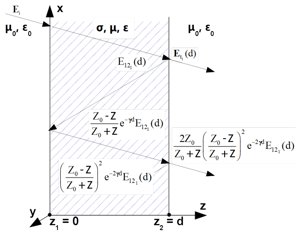
The incident wave [latex]{\bf E}_{{12}_1}(z)[/latex] by passage for the first time to the interface [latex]z_2 =d[/latex] is determined with Eq. (5.36). One part of this field [latex]{\bf E}_{t_1}(d)[/latex] is transmitted outside the shield according to Eq. (5.37). The rest is reflected according to the reflection coefficient [latex]\bf \Gamma^E[/latex] determined with Eq. ([Gamma]). This field propagating backwards to the left interface suffers attenuation and phase shift
[latex]\frac{Z_0 - {\bf Z} }{Z_0 + {\bf Z}} e^{{\bf{\gamma }} (z -d) } {\bf E}_{{12}_1}(d)[/latex]
This field by reaching the left barrier by [latex]z = 0[/latex] reflects again according to the reflection coefficient [latex]\bf \Gamma^E[/latex] determined with Eq. ([Gamma]) and propagates forward suffering attenuation and phase shift
[latex]\left (\frac{Z_0 - {\bf Z} }{Z_0 + {\bf Z}} \right)^2 e^{-{\bf{\gamma }} d } e^{-{\bf{\gamma }} z } {\bf E}_{{12}_1}(d)[/latex]
Part of the field according to transmission coefficient [latex]{\bf T}^E[/latex] presented in Eq. (5.27) leaves the barrier
[latex]{\bf E}_{t_2} (d)= \frac{2 Z_0 } {Z_0+ {\bf Z}} \left (\frac{Z_0 - {\bf Z} }{Z_0 + {\bf Z}} \right)^2 e^{-2{\bf{\gamma }} d } {\bf E}_{{12}_1}(d) \label{E12_2t}\tag{5.44}[/latex]
The rest is reflected for the third time. This process repeats infinitely.
By introduction of the term
[latex]\bf \Delta = \frac{Z_0 - {\bf Z} }{Z_0 + {\bf Z}} \cdot e^{-{\bf{\gamma }} d }[/latex]
transmitted fields is following sum
[latex]{\bf E}_{t} (d) = \frac{4 {\bf Z} Z_0 } {\left (Z_0+ {\bf Z}\right)^2} \cdot e^{-{\bf{\gamma }} d} \cdot \left( 1 + \bf \Delta^2 + \bf \Delta^4 + \cdots \right) \cdot {\bf E}_i (0)[/latex]
For [latex]|\bf \Delta | < 1[/latex] following relation is valid [latex]1 + \bf \Delta^2 + \bf \Delta^4 + \cdots = \frac{1}{1 - \bf \Delta^2 }[/latex] Finally, relation [latex]{\bf E}_i (0) / {\bf E}_t(d)[/latex] is identical as presented with Eq. (5.33) (q.e.d.)!. Derivation of the shield effectiveness for magnetic field [latex]SE^H(p)[/latex] gives the same results. Memorise that, shield effectiveness of electric and magnetic field in the far field zone is identical regardless thickness [latex]d[/latex] of the shielding barrier, although sequence of stages is different. In case of electric field majority of shielding effectiveness stems from reflection at the left surface [latex]z_1 = 0[/latex]. Reflection coefficient [latex]{\bf \Gamma}^E[/latex] there is ruled with Eq. (5.19)11. Contrariwise there is rather amplification instead of reflection of magnetic field at this surface, since according to Eq. (5.19) [latex]{\bf \Gamma}^H \approx 1[/latex]. In consequence magnetic field transmitted to the shield material is almost doubled, see [latex]{\bf T}^H[/latex] in Eq. (5.20). By passage from the left to the right interface electric and magnetic fields are attenuated in the same way according to attenuation coefficient [latex]{\bf \gamma}[/latex]. At the right interface roles of electric and magnetic fields swap. Electric field is barely reflected and almost double field is transmitted outside. On the contrary magnetic field is almost totally reflected.
Another situation is if the shield is situated in the near field zone of electric or magnetic radiator. Reflection coefficient [latex]{\bf \Gamma}^E[/latex] and [latex]{\bf \Gamma}^H[/latex] and transmission coefficients [latex]{\bf T}^E[/latex] and [latex]{\bf T}^H[/latex] at the left interface of the shield, [latex]z_1 = 0[/latex] are ruled with Eq. (5.19) and Eq. (5.20) respectively. At the right interface, by [latex]z_2 = d[/latex] they obey Eq. (5.26) and Eq. (5.27) respectively.
In case of near field zone intrinsic impedance [latex]Z_0[/latex] in above mentioned formulas must be replaced with the wave impedance [latex]{\bf{Z}}_w[/latex], defined with Eq. ([Zw]). In case of electrical radiator the wave impedance in the near field zone is much bigger than intrinsic impedance [latex]Z_0[/latex] of the medium and in case of magnetic radiator much smaller, as can be drawn from Fig.[Zw_em_Fig].
By electrical radiator replacement of [latex]Z_0[/latex] with [latex]{\bf{Z}}_w[/latex] only slightly increases shielding effectiveness because already by [latex]Z_0 = 377[/latex] [latex]\Omega[/latex] [latex]{\bf \Gamma}^E[/latex] is practically equal [latex]-1[/latex] and [latex]{\bf T}^E[/latex] equal [latex]0[/latex] at the interface [latex]z_1 = 0[/latex]12. Thickness [latex]d[/latex] of shielding material is irrelevant.
There is another scenario by magnetic radiator. [latex]{\bf{Z}}_w[/latex] is comparable with intrinsic impedance [latex]\bf Z[/latex] of shielding material. In consequence there is good impedance matching at the interface [latex]z_1 = 0[/latex] as well at the interface [latex]z_2 = d[/latex], compare explanation in chapter [impedance maching]. Relatively much field is transferred to the shield at the interface [latex]z_1 = 0[/latex] and from the shield at the interface [latex]z_2 = d[/latex]. Shielding effect is mainly due to attenuation in the shielding material. Therefore thickness [latex]d[/latex] of shield material is crucial.
Feed-throughs and apertures in RF shields
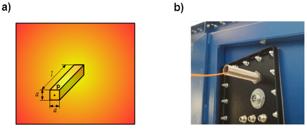
Shielding enclosures must have in many applications possibility of transferring optical signals with glass fibre and media such as gas, compressed air, water supply, waste water. In order not to deteriorate shielding effectiveness feed-troughs are indispensable. Feed-through is simply a wave guide as presented in chapter [wave-guides]. It can have square, circular as shown in Fig. 5.27 or polygonal cross-section.

[latex]{\bf{E}}_z[/latex] component is defined with Eq. ([gamma_z]). For frequencies below cut-off attenuation coefficient [latex]{\bf \gamma}_{z,mn}[/latex] defined with the first row of Eq. ([gamma_z2]) is real and is noted here with [latex]\alpha_{z,mn}[/latex]
[latex]{\bf{\alpha}}_{z,mn} = \frac{\omega}{v_0}\sqrt{ \left(\frac{f_{c,mn}}{f} \right)^2 - 1} \label{alpha_z}\tag{5.48}[/latex]
Assuming that the frequency is much less than the cutoff frequency for the mode, [latex]\alpha_{z,mn}[/latex] simplifies to
[latex]{\bf{\alpha}}_{z,mn} \approx \frac{2 \pi f_{c,mn} } {v_0} \label{alpha_z1}\tag{5.49}[/latex]
Substituting the relation for the cut-off frequency for the lowest-order [latex]TE_{10}[/latex] mode given in Eq. ( [gamma_zz]) [latex]f_{c,10} = v_0/2a[/latex] gives [latex]{\bf{\alpha}}_{z,10} \approx \pi / a[/latex]. Finally shielding effectiveness in [latex]dB[/latex] yields
[latex]SE^E_{dB}(p) = 20 \cdot \log \left[ e^{\alpha_{z,10}l} \right] = 20 \cdot \pi \cdot \log [e] \cdot \frac{ l}{a} \approx 27.3 \cdot \frac{l}{a} \label{SE_feedthrough}\tag{5.50}[/latex]
Concluding: in order to ensure attenuation of the feed-through bigger than [latex]100[/latex] [latex]dB[/latex], relation of its length [latex]l[/latex] to cross-sectional dimension [latex]a[/latex] should be bigger than [latex]4[/latex].

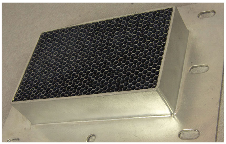
Ventilation aperture are usually mantled with honeycomb grid as shown in Fig. 5.28. It is just matrix of feed-throughs with hexagonal cross-section.
- By neglecting the leakage field.↩︎
- Number of turns is determined with the number of conductor passages through the hole.↩︎
- Protected are ports of any network like: power mains, ethernet, telecommunication, cable TV etc..↩︎
- Proportionality in the plot is deformed in order to make visible all discharge regimes.↩︎
- According to [@Hammond] for good conducting materials (metals) holds inequality [latex]\epsilon / \sigma \ll 1 s[/latex].↩︎
- This explains why magnetic monopoles do not exist.↩︎
- Mind that [latex]\overrightarrow{E}[/latex] represents total field i.e. due to all charges: free charges at the metal plates and polarization charges of dipoles in material.↩︎
- Mind that [latex]\overrightarrow{B}[/latex] represents total field i.e. due to all currents: conducted current driven in the metal bars and magnetisation current in material.↩︎
- The second Maxwell’s equation rules magnetic field originating from current [latex]\mathop{\mathrm{rot}}{\overrightarrow{\bf{H}}} = \sigma \overrightarrow{\bf{E}} + j \omega \epsilon \overrightarrow{\bf{E}}[/latex]. Current can be conducted or can be due to dielectric attribute of material named the displacement current.↩︎
- Any exponential function with imaginary operator j in exponent such as [latex]e^{j \frac{d}{\delta}}[/latex] has constant module equal [latex]1[/latex] and is responsible only for phase shifting.↩︎
- [latex]{\bf \Gamma}^E \approx -1[/latex] because [latex]{\bf{Z}} \ll Z_0[/latex]↩︎
- Remind that in case of static field shielding would happen totally at the interface [latex]z_1 = 0[/latex] and other side of the shield would be free of any electric field.↩︎