
SWITCHING OFF DC WITH USE OF TRANSISTOR
Tadeusz Daszczyński; Waldemar Chmielak; and Zbigniew Pochanke
SWITCHING OFF DC WITH USE OF TRANSISTOR
Introduction
Semiconductor connectors are characterized by important advantages in relation to the contact switches. The switching process is implemented in them by changing the conductivity of the semiconductor connectors, and not, as is the case in the contact switches, by mechanical joining or separation of the contacts. When switching off, there is no problem to quench the arc, and then to rebuild the electrical strength of the pit channel. When switching on, there is no problem in welding or melting the contacts. The reliability of electronic components is much easier to achieve than in the case of complex mechanical devices, such as contact switches. They are also characterized by far greater, virtually unlimited, connection durability and connection speed. The electronic structure of semiconductor switches is a strong motivation for replacing them with contact switches wherever possible, i.e. where the maximum overvoltage and overcurrent values do not exceed the permissible values for semiconductor connectors.
An important disadvantage of semiconductor switches, which prevents such a procedure, is their high inter-clamp resistance, which exceeds the magnitude of inter-clamp resistance of the contact switches, and leads to an increased release of thermal energy during the conductive current through the switch. This energy should not only be dissipate, but, above all, the customer has to pay for it. In addition, semiconductor switches are not in the state of open galvanic break in the circuit and require complex means to protect them against the consequences of switching processes, for which they are very sensitive. Semiconductor switches are currently only installed in such cases in which the benefits of their electronic construction outweigh the losses resulting from their high clamping resistance and the costs of necessary circuits and additional devices.
An example of a system in which semiconductor switches are used, is a 3 kV direct current network (in Poland it is the PKP electric traction network), HVDC network (200 – 1100 kV), generators excitation (10 – 30 kV), or alternative sources energy (from several to several thousand volts). In this network, direct current creates difficult switching conditions for contact switches, due to the lack of a natural transition of the current through a zero value. It results in the necessity of forcing the passage of current through zero, which at high voltage is an extremely thankless task. Under such conditions, the contact switches are successfully replaced by semiconductor switches.
Transistors IGBT
The Insulated Gate Bipolar Transistor (IGBT) is a minority-carrier device with high input impedance and large bipolar current-carrying capability. Many designers view IGBT as a device with MOS input characteristics and bipolar output characteristic that is a voltage-controlled bipolar device. To make use of the advantages of both Power MOSFET and BJT, the IGBT has been introduced. It’s a functional integration of Power MOSFET and BJT devices in monolithic form. It combines the best attributes of both to achieve optimal device characteristics.
The IGBT is suitable for many applications in power electronics, especially in Pulse Width Modulated (PWM) servo and three-phase drives requiring high dynamic range control and low noise. It also can be used in Uninterruptible Power Supplies (UPS), Switched-Mode Power Supplies (SMPS), and other power circuits requiring high switch repetition rates. IGBT improves dynamic performance and efficiency and reduced the level of audible noise. It is equally suitable in resonant-mode converter circuits. Optimized IGBT is available for both low conduction loss and low switching loss. The main advantages of IGBT over a Power MOSFET and a BJT are:
- It has a very low on-state voltage drop due to conductivity modulation and has superior on-state current density. So smaller chip size is possible and the cost can be reduced.
- Low driving power and a simple drive circuit due to the input MOS gate structure. It can be easily controlled as compared to current controlled devices (thyristor, BJT) in high voltage and high current applications.
- Wide SOA. It has superior current conduction capability compared with the bipolar transistor. It also has excellent forward and reverse blocking capabilities.
The main drawbacks are:
- Switching speed is inferior to that of a Power MOSFET and superior to that of a BJT. The collector current tailing due to the minority carrier causes the turn-off speed to be slow.
- There is a possibility of latchup due to the internal PNPN thyristor structure.
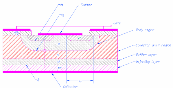
The basic structure of IGBT was shown on Fig. 1.
During the experiment the IGBT model PM600HSA120 (Fig. 2) will be used.
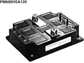
The main nominal parameters of the IGBT model PM600HSA120:
- max voltage – 1200 V
- max current – 600 A
- max frequency – 20 kHz
- max switching off time – 3,5 s
- switching time – 0,5-3,5 s
- max power of losses – 3470 W
- max temperaturę – 150⁰C
- overload current – 740-1000 A
- short-circuit current – higher than 1000 A
- time delay of overload signal – 5 s
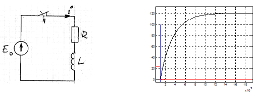
The laboratory setup
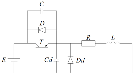
The laboratory setup scheme is shown on Fig. 3.
Simulation model
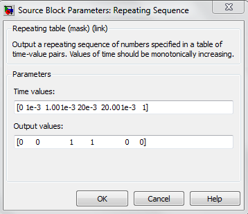
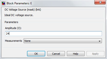
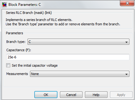
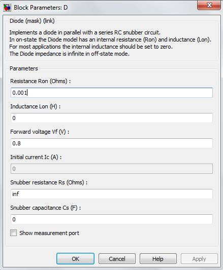
The Simulink model of a switching process with use of IGBT is shown on Fig. 43.
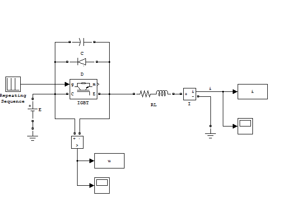
The model was built from the blocks:
1) ‘Repeating sequence’ – Simulink/Sources
2) DC Voltage Source
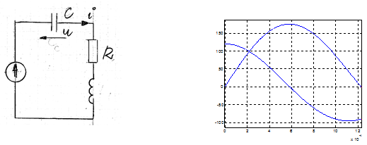
3) Capacitor – Series RLC branch
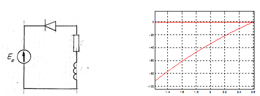
4) Diode
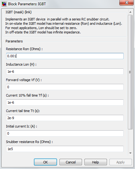
5) IGBT
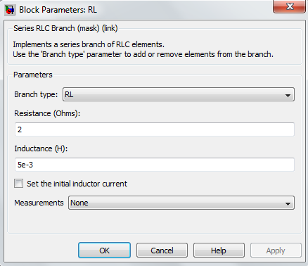
6) Load RL – Series RLC branch
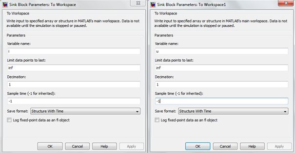
7) Sink block parameters – To workspace
Matlab script to work with Simulink was added in the end of this instruction.
During the exercise both the voltage and current are observed on oscilloscope. On Fig. 5 the voltage and current versus time was shown. On Fig. 6 the voltage and current versus time was shown with markers.
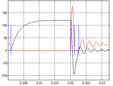
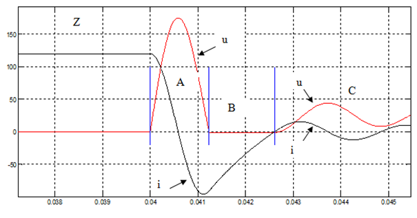
On Fig. 6 the four switching processes are shown and can be described:
1) Process Z – switching on the load
Current equation:
$$L\frac{di}{dt}+Ri={{E}_{o}}$$, from zero initial conditions
Current transform:
$$I\left( s \right)=\frac{{{E}_{o}}}{s\left( Ls+R \right)}$$
2) Process A – switching off the transistor: from cutting off current in transistor to the moment of zero voltage on switching capacitance
Current and voltage equations:
$$L\frac{di}{dt}+Ri+u={{E}_{o}}$$
$$C\frac{du}{dt}=i $$
for initial conditions: $$i\left( 0 \right)={{I}_{A0}}=\frac{{{E}_{o}}}{R};u\left( 0 \right)=0$$,
Equations are valid up to the moment $${{t}_{Ae}}:u\left( {{t}_{Ae}} \right)=0$$
Voltage transform:
$$U\left( s \right)=\frac{{{E}_{o}}}{s\left( LC{{s}^{2}}+RCs+1 \right)}+\frac{L{{I}_{A0}}}{LC{{s}^{2}}+RCs+1}$$
3) Process B – dissipation of magnetic energy: from the moment of zero voltage on switching capacitance (diode D starts conducting) up to the moment of termination of conduction through the diode D
Current equation:
$$L\frac{di}{dt}+Ri={{E}_{o}}$$, przy $$I\left( 0 \right)={{I}_{Ae}}$$ – the current in the inductance at the end of the A process
Equation are valid up to the moment $${{t}_{Be}}:i\left( {{t}_{Be}} \right)=0$$
Current transform:
$$I\left( s \right)=\frac{{{E}_{o}}}{s\left( Ls+R \right)}+\frac{L{{I}_{Ae}}}{Ls+R}$$
4) Process C – reconstruction of the source voltage on the connector terminals: from the moment of termination of the conduction through the diode D to the component decay on the recovery voltage
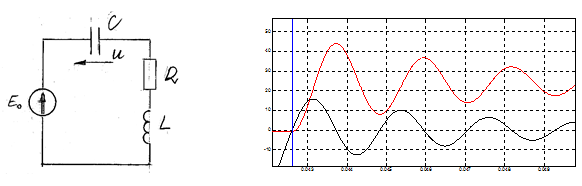
Current and voltage equations:
$$L\frac{di}{dt}+Ri+u={{E}_{o}}$$
$$C\frac{du}{dt}=i $$
for zero initial conditions Voltage transform:
$$U\left( s \right)=\frac{{{E}_{o}}}{s\left( LC{{s}^{2}}+RCs+1 \right)}$$
MATLAB program for simulation
clear all;close all;clcsim('igbt_instr'); % name of the Simulink scheme t = u.time; u = u.signals.values; i = i.signals.values;% basic oscillograms clf; plot(t,u,'r',t,10*i,'k');grid;